

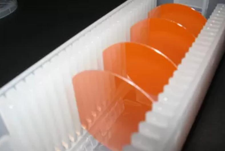
2 Inch Gallium Phosphide Crystal Substrate GaP Wafer 0.3 Thickness Lapped Surface
Gallium phosphide (GaP), a phosphide of gallium, is a c […]
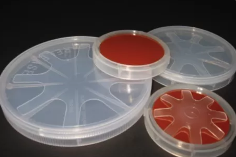

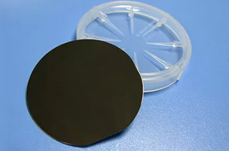
Gallium phosphide (GaP), a phosphide of gallium, is a compound semiconductor material with an indirect band gap of 2.26eV(300K). The polycrystalline material has the appearance of pale orange pieces. Undoped single crystal wafers appear clear orange, but strongly doped wafers appear darker due to free-carrier absorption. It is odorless and insoluble in water.Sulfur or tellurium are used as dopants to produce n-type semiconductors. Zinc is used as a dopant for the p-type semiconductor.Gallium phosphide has applications in optical systems. Its refractive index is between 4.30 at 262 nm (UV), 3.45 at 550 nm (green) and 3.19 at 840 nm (IR).
Gallium Phosphide Crystal Substrate Product Specification
| Growth | LEC |
|---|---|
| Diameter | Ø 2″ |
| Thickness | 300um |
| Orientation | <100> / <111> / <110> or others |
| Off orientation | Off 2° to 10° |
| Surface | One side polished or two sides polished or lapped |
| Flat options | EJ or SEMI. Std . |
| TTV | <= 10 um |
| EPD | <= 2E5 cm-2 |
| Grade | Epi polished grade / mechanical grade |
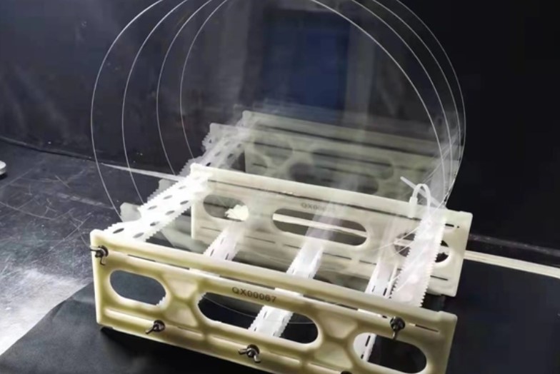
| Package | Single wafer container |
| Dopant available | S / Zn / Cr / Undoped |
|---|---|
| Type of conductivity | N / P ,Semi-conducting / Semi-insulating |
| Concentration | 1E17 – 2E18 cm-3 |
| Mobility | > 100 cm2 / v.s. |
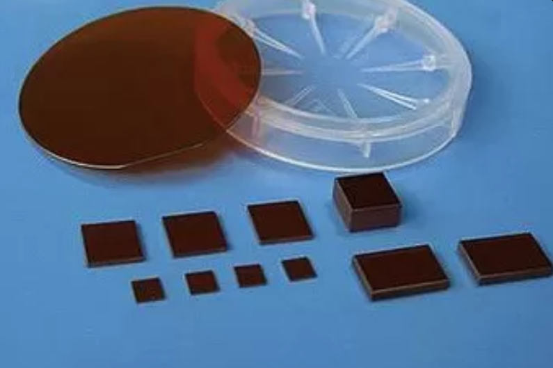
high quality single crystal GaP wafer ( Gallium phosphide ) to electronic and optoelectronic industry in diameter up to 2 inch . Gallium phosphide ( GaP ) crystal is an orange-yellow semi-translucent material formed by two elements , GaP wafer is an important semiconductor material which have unique electrical properties as other III-V compound materials and is widely used as red , yellow , and green LED ( light-emitting diodes ) . We have as-cut single crystal GaP wafer for your LPE application , and also provide epi ready grade GaP wafer for your MOCVD & MBE epitaxial application . Please contact us for more product information.
| Product Name: | Gallium phosphide (GaP) crystal substrate |
| Technical parameters: | Crystal structure Cubic a = 5.4505 Å Growth method Czochralski method Density 4.13 g / cm 3 Mp 1480 o C 1 Thermal expansion coefficient 5.3 x10 -6 / O C Dopant S-doped undoped Direction <111> or <100> <100> or <111> Type N N Thermal Conductivity 2 ~ 8 x10 17 / cm 3 4 ~ 6 x10 16 / cm 3 Resistivity W.cm 0.03 to 0.3 EPD (cm -2) <3×10 5 <3×10 5 |
| Specifications: | Crystallographic directions <111>, <100> ± 0.5 o Standard polished Size Ø2 “* 0.35mm; Ø2” * 0.43mm. Ø3″x0.3mm Note according to customer requirements with special dimensions and orientation substrates |
| StandardPacking | 1000 clean room, 100 clean bag or single box packaging |
FAQ:
Q: What’s the delivery time?
A: (1) For the standard products
For inventory: the delivery is 5 workdays after you place the order.
For customized products: the delivery is 2 or 3 weeks after you place the order.
(2) For the special-shaped products, the delivery is 4 workweeks after you place the order.
Q: What’s your MOQ?
A: (1) For inventory, the MOQ is 3pcs.
(2) For customized products, the MOQ is 10-20pcs up.
Related Products
Send Inquiry
