


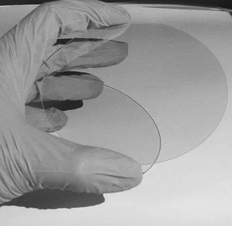
2Inch 4inch free-standing GaN Gallium Nitride Wafer
Name: GaN Callium Nitride Wafer Application: LED Suppli […]
Name: GaN Callium Nitride Wafer
Application: LED
Supplier: Shanghai Xinkehui
Size: 2 inch or custom size
Moq: 5 pcs
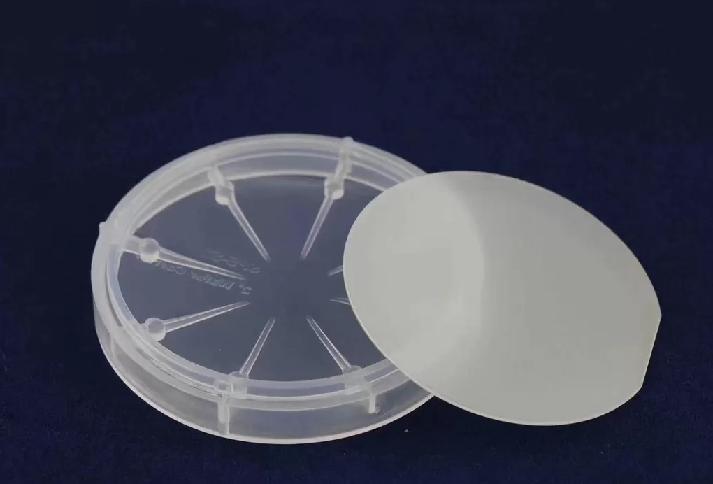
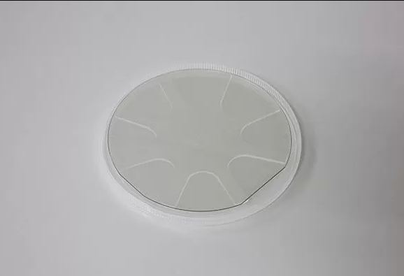
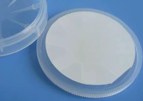
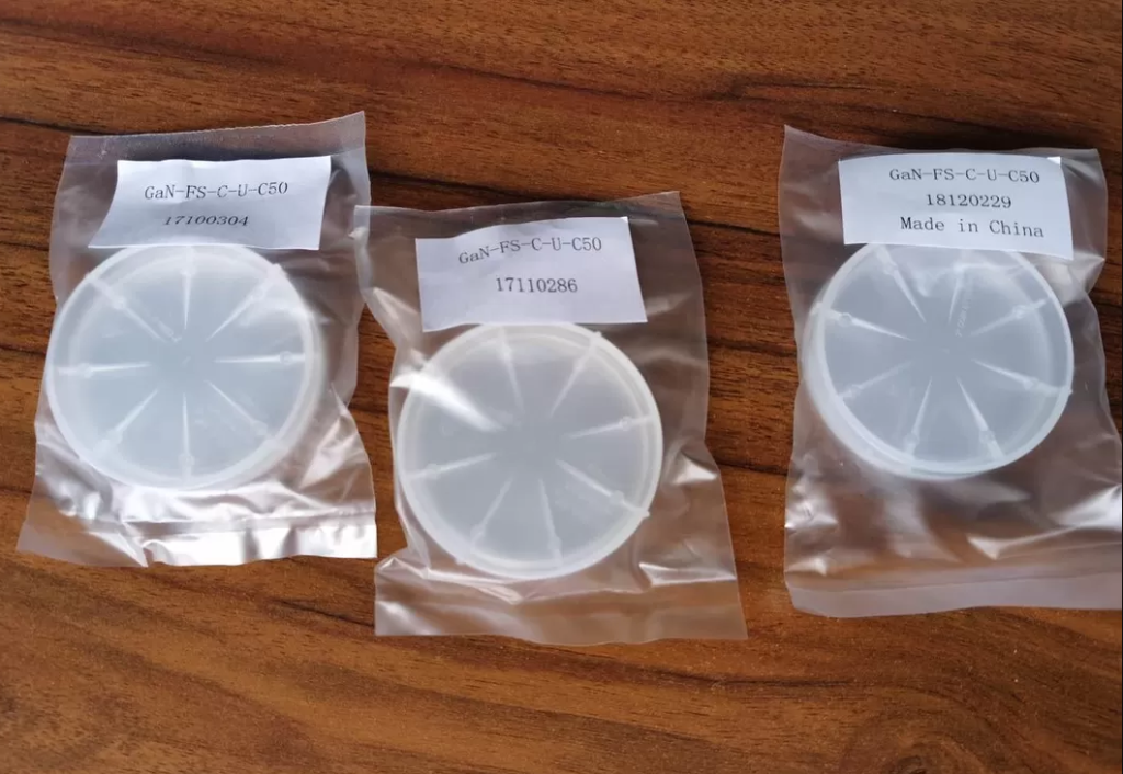
Packing details: single wafer case by vacuum package
Delivery time: 1-5 weeks
2inch GaN substrates template,GaN wafer for LeD,semiconducting Gallium Nitride Wafer for ld,GaN template, mocvd GaN Wafer,Free-standing GaN Substrates by Customized size,small size GaN wafer for LED, mocvd Gallium Nitride wafer 10x10mm,5x5mm, 10x5mm GaN wafer,Non-Polar Freestanding GaN Substrates(a-plane and m-plane)
2inch 1um 4um thickness GaN AlGaN AlN layer template by MOCVD on SSP 430um sapphire substrates
Application of GaN wafer
GaN can be used in many areas such as LED display, High-energy Detection and Imaging,
Laser Projection Display, Power Device, etc.
- Laser Projection Display, Power Device, etc. Date storage
- Energy-efficient lighting Full color fla display
- Laser Projecttions High- Efficiency Electronic devices
- High- Frequency Microwave Devices High-energy Detection and imagine
- New energy solor hydrogen technology Environment Detection and biological medicine
- Light source terahertz band


GaN Wafer Characteristic
- III-Nitride(GaN,AlN,InN)
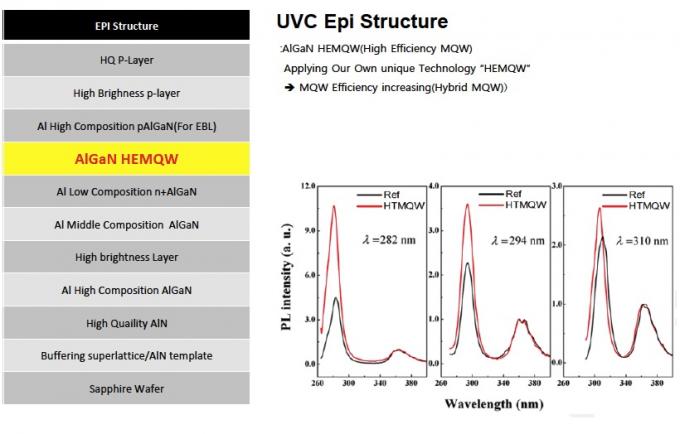
Gallium Nitride is one kind of wide-gap compound semiconductors. Gallium Nitride (GaN) substrate is
a high-quality single-crystal substrate. It is made with original HVPE method and wafer processing technology, which has been originally developed for 10+years in China. The features are high crystalline, good uniformity, and superior surface quality. GaN substrates are used for many kinds of applications, for white LED and LD(violet, blue and green) Furthermore, development has progressed for power and high frequency electronic device applications.
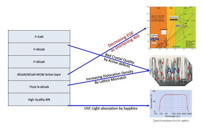
Forbidden band width (light emitting and absorption) cover the ultraviolet, visible light and infrared.
GaN Wafer Packing Details
Shanghai Xinkehui New Material GaN Supplier Enterprise Vision
we will provide high quality GaN substrate and application technology for the industry with our factory.
High quality GaNmaterial is the restraining factor for the III-nitrides application, e.g. long life
and high stability LDs, high power and high reliability micro-wave devices, High brightness
and high efficiency, energy-saving LED.
Send Inquiry
