

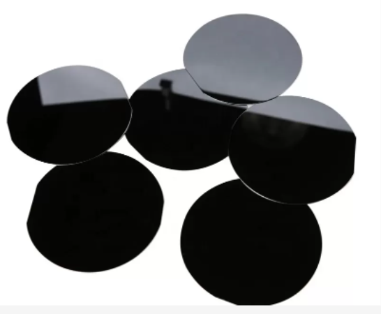
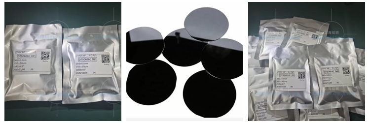
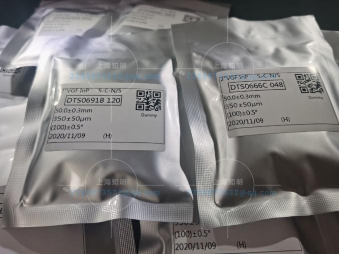
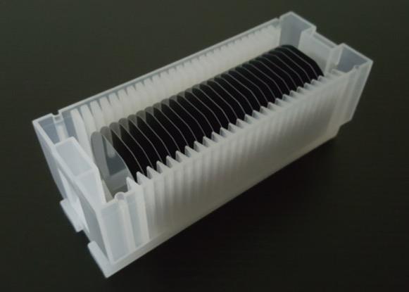
3 Inch InP Crystal Dummy Prime Semiconductor Substrate
growth (modified VFG method) is used to pull a sin […]
growth (modified VFG method) is used to pull a single crystal through a boric oxide liquid encapsulant starting from a seed.
The dopant (Fe, S, Sn or Zn)is added to the crucible along with the polycrystal. High pressure is applied inside the chamber to prevent decomposition of the Indium Phosphide.he company has developed a process to yield fully stoechiometric, high purity and low dislocation density inP single crystal.
The VFG technique improves upon the LEC method thanks to a thermal baffle technology in connection with a numerical
modeling of thermal growth conditions. tCZ is a cost-effective mature technology with high quality reproducibility from boule to boule.
It has the advantages of high electronic limit drift speed, good radiation resistance and good heat conduction. Suitable for manufacturing high-frequency, high-speed, high-power microwave devices and integrated circuits.
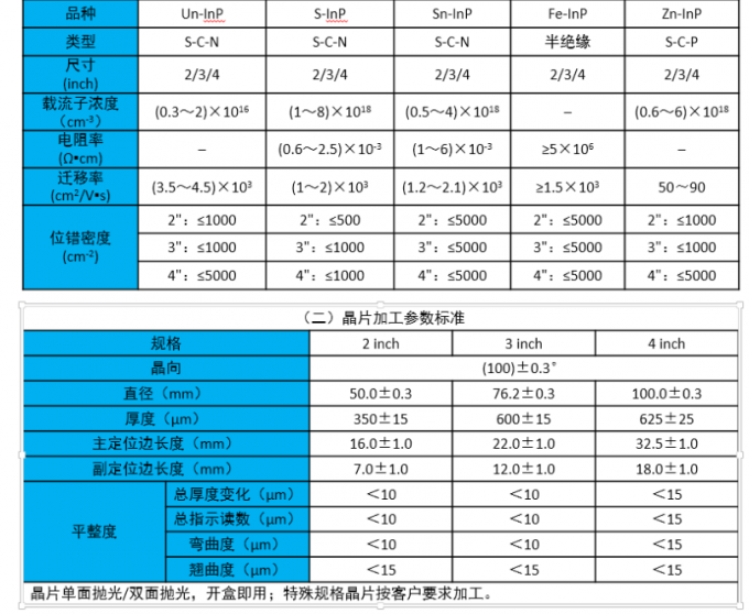
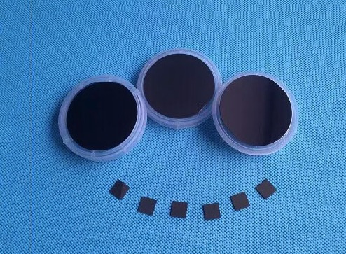
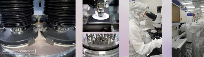
1, The crystal is grown by liquid-sealed straight-drawing technology (LEC), with mature technology and stable electrical performance.
2, using X-ray directional instrument for precise orientation, the crystal orientation deviation is only ±0.5°
3, the wafer is polished by chemical mechanical polishing (CMP) technology, surface roughness <0.5nm;
4, to achieve the “open box ready to use” requirement;
5, according to user requirements, special specifications product processing.
—FAQ –
Q: Are you trading company or manufacturer ?
A: Shanghai XInkehui New Material is a trading company but have a sapphire manufacturer
as a supplier of semiconductor materials wafers for a wide span of applications.
Q: How long is your delivery time?
A: Generally it is 5-10 days if the goods are in stock. or it is 15-20 days if the goods are not
in stock,it is according to quantity.
Q: Do you provide samples ? is it free or extra ?
A: Yes, we could offer the sample for free charge but do not pay the cost of freight.
Q: What is your terms of payment ?
A: Payment<=1000USD, 100% in advance. Payment>=1000USD,
50% T/T in advance ,balance before shippment.
If you have another question, pls feel free to contact us as below:
Send Inquiry
