

6 Inch N Type Polished Silicon Wafer DSP SiO2 Silicon Oxide Wafer
Polished Silicon Wafer High-purity (11N) 1-12 inch sing […]
Polished Silicon Wafer High-purity (11N) 1-12 inch single- and double-polished Czochralski wafers
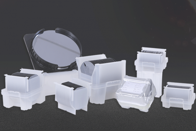
Sizes 1″ 2″ 3″ 4″ 5″ 6″ 8″ 12″ and special size and specification wafers
Surface Single polishing disc, double polishing disc, abrasive disc, corrosion disc, cutting disc
Crystal orientation <100> <111> <110> <211> <511> and silicon wafers with various off-angles
Thickness 100um 200um 300um 400um 500um 1mm 5mm and other thicknesses, thickness tolerance +-10um,
TTV< 10um or according to customer requirements, roughness <0.2nm
Conductivity type N-type, P-type, undope (intrinsically high resistance)
Single crystal method Czochralski (CZ), zone melting (FZ), NTD (middle photo)
Resistivity Re-doping can reach <0.001 ohm.cm, low-doping conventional 1~10 ohm.com, medium-light conventional 500~800 ohm.cm,
zone melting intrinsic: > 1000 ohm.cm, >3000 ohm.cm, >5000 ohm.cm, >8000 ohm.cm, >10000 ohm.cm
Process parameters Flatness TIR: ≤3μm, Warpage TTV: ≤10μm,
Bow/Warp≤40μm, roughness≤0.5nm, particle size <≤10ea@ > 0.3μ)
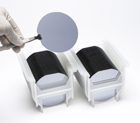
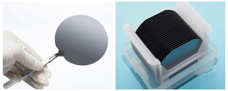
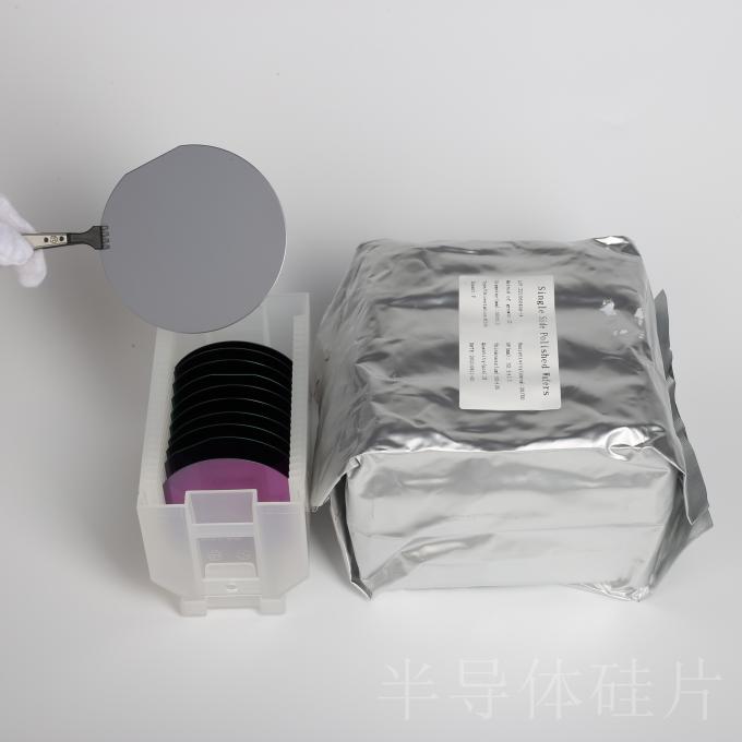
Packing method Ultra-clean aluminum foil vacuum packaging 10 pieces, 25 pieces
Processing customization The processing time of model, crystal orientation, thickness, resistivity, etc. is slightly different according to different specifications and parameters.
Application introduction It is used for synchrotron radiation sample carriers such as processes, PVD/CVD coatings as substrates, magnetron sputtering growth samples, XRD, SEM,
Atomic force, infrared spectroscopy, fluorescence spectroscopy and other analysis test substrates, molecular beam epitaxy growth substrates, X-ray analysis of crystalline semiconductors
Special statement: All silicon wafers of our company are processed from single crystal silicon drawn from native polysilicon, not cheap recycled silicon wafers or used re-polished silicon wafers! The quotation includes a 16% VAT invoice.
| Straight Pull Single Side Polished Silicon Wafer |
| 1 inch (25.4mm) single-sided polished Czochralski wafer thickness 500um 2 inches (50.8mm) single-sided polished Czochralski wafer thickness 280um 3 inches (76.2mm) single-sided polished Czochralski wafer thickness 380um 4-inch (100mm) single-sided polished straight-pull silicon wafer with a thickness of 500um 5-inch (125mm) single-sided polished Czochralski wafer thickness 625um 6 inches (150mm) single-sided polished Czochralski wafer thickness 675um |
| Czochralski double-sided polished silicon wafers |
| 1 inch (25.4mm) double-sided polished Czochralski wafer thickness 500um 2 inches (50.8mm) double-sided polished Czochralski wafer thickness 280um 3 inches (76.2mm) double-sided polished Czochralski wafer thickness 380um 4 inches (100mm) double-sided polished Czochralski wafer thickness 500um 5 inches (125mm) double-sided polished Czochralski wafer thickness 625um 6 inches (150mm) double-sided polished Czochralski wafer thickness 675um |
| Straight-pulled single-sided polished ultra-thin silicon wafers |
| 1 inch (25.4mm) single-sided polished ultra-thin straight-pull silicon wafer thickness 100um 2 inches (50.8mm) single-side polished ultra-thin straight-pull silicon wafer thickness 100um 3 inches (76.2mm) single-side polished ultra-thin straight-pull silicon wafer thickness 100um 4-inch (100mm) single-sided polished ultra-thin straight-pull silicon wafer with a thickness of 100um |
| Czochralski double-sided polished ultra-thin silicon wafers |
| 1 inch (25.4mm) double-sided polished ultra-thin Czochralski wafer thickness 100um 2 inches (50.8mm) double-sided polished ultra-thin Czochralski wafer thickness 100um 3 inches (76.2mm) double-sided polished ultra-thin Czochralski wafer thickness 100um 4 inches (100mm) double-sided polished ultra-thin Czochralski wafer thickness 100um |
| Zone melting single-side polished silicon wafer |
| 1-inch (25.4mm) fused silicon wafer thickness 500um in single-sided polishing area 2 inches (50.8mm) fused silicon wafer thickness 280um in single-side polishing area 3-inch (76.2mm) fused silicon wafer thickness 380um in single-side polishing area 4 inches (100mm) fused silicon wafer thickness 500um in single-side polishing area |
| Zone melting double-sided polished silicon wafers |
| 1 inch (25.4mm) fused silicon wafer thickness 500um in double-sided polishing area 2 inches (50.8mm) fused silicon wafer thickness 280um in double-sided polishing area 3-inch (76.2mm) fused silicon wafer thickness 380um in double-sided polishing area 4 inches (100mm) fused silicon wafer thickness 500um in double-sided polishing area |
| Zone melting single-side polished ultra-thin silicon wafer |
| 1-inch (25.4mm) single-sided polishing zone melting ultra-thin silicon wafer thickness 100um 2 inches (50.8mm) single-sided polishing zone melting ultra-thin silicon wafer thickness 100um 3 inches (76.2mm) single-sided polishing zone melting ultra-thin silicon wafer thickness 100um 4 inches (100mm) single-sided polishing zone melting ultra-thin silicon wafer thickness 100um |
| Zone melting double-sided polished ultra-thin silicon wafers |
| 1 inch (25.4mm) double-sided polishing area melting ultra-thin silicon wafer thickness 100um 2 inches (50.8mm) double-sided polishing area melting ultra-thin silicon wafer thickness 100um 3 inches (76.2mm) double-sided polishing area melting ultra-thin silicon wafer thickness 100um 4 inches (100mm) double-sided polishing area melting ultra-thin silicon wafer thickness 100um |
Send Inquiry
