

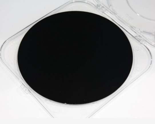
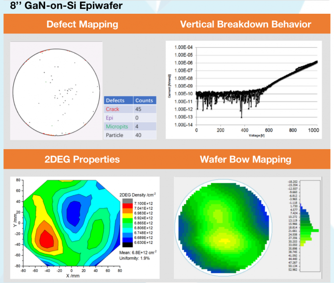
8″ dia200mm GaN-on-Si Epi-wafer for Micro-LED 6inch AlGaN/GaN HEMT-on-HR Si Epi wafer
Gallium Nitride is one kind of wide-gap compound semico […]
Gallium Nitride is one kind of wide-gap compound semiconductors. Gallium Nitride (GaN) substrate is
a high-quality single-crystal substrate. It is made with original HVPE method and wafer processing technology, which has been originally developed for 10+years in China. The features are high crystalline, good uniformity, and superior surface quality. GaN substrates are used for many kinds of applications, for white LED and LD(violet, blue and green) Furthermore, development has progressed for power and high frequency electronic device applications.
| Items | Values/Scope |
| Substrate | Si |
| Wafer diameter | 4” / 6” / 8” |
| Epi-layer thickness | 4-5 μm |
| Wafer bow | <30 μm, Typical |
| Surface Morphology | RMS<0.5nm in 5×5 μm² |
| Barrier | AlXGa1-XN, 0<X<1 |
| Cap layer | In-situ SiN or GaN (D-mode); p-GaN (E-mode) |
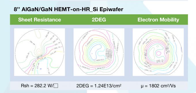
| 2DEG density | >9E12/cm2 (20nm Al0.25GaN) |
| Electron mobility | >1800 cm2/Vs (20nm Al0.25GaN) |
| Items | Values/Scope |
| Substrate | HR_Si / SiC |
| Wafer diameter | 4’’/6’’ for SiC, 4”/ 6”/ 8” for HR_Si |
| Epi-layer thickness | 2-3 μm |
| Wafer bow | <30 μm, Typical |
| Surface Morphology | RMS<0.5nm in 5×5 μm² |
| Barrier | AlGaN or AlN or InAlN |
| Cap layer | In-situ SiN or GaN |
| Items | GaN-on-Si | GaN-on-Sapphire |
| 4”/ 6”/ 8” | 2”/ 4”/ 6” | |
| Epi-layer Thickness | <4 μm | <7 μm |
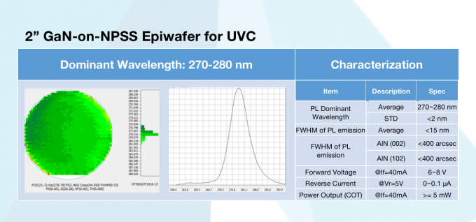
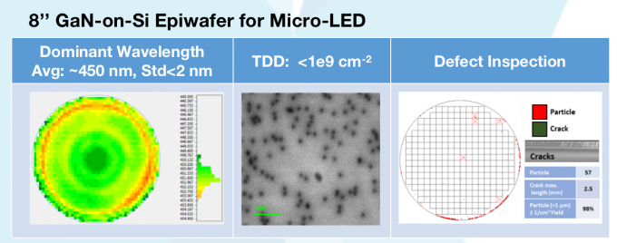
| Average Dominant/ Peak Wavelength | 400-420nm, 440-460nm, 510-530nm | 270-280nm, 440-460nm, 510-530nm |
| FWHM | <20nm for Blue/Near-UV<40nm for Green | <15nm for UVC<25nm for Blue<40nm for Green |
| Wafer Bow | <50 μm | <180 μm |
FAQ
Q: What you can supply logistics and cost?
(1) We accept DHL, Fedex, TNT, UPS, EMS, SF and etc.
(2) If you have your own express number, it’s great.
If not, we could assist you to deliver. Freight=USD25.0(the first weight) + USD12.0/kg
Q: What’s the delivery time?
(1) For the standard products such as 2inch 0.33mm wafer.
For inventory: the delivery is 5 workdays after order.
For customized products: the delivery is 2 or 4 workweeks after order.
Q: How to pay?
100%T/T, Paypal, West Union, MoneyGram, Secure payment and Trade Assurance.
Send Inquiry
