

Dia 50.8mm Ge Wafers Semiconductor Substrate Ga Doped Substrate N Type 500 um
Ge wafer for microelectronic application N type,&n […]
Ge wafer for microelectronic application
| N type, Sb doped Ge wafer |
| N type,undoped Ge wafer |
| P type,Ga doped Ge wafer |
| Available size:2”-6” |
| Available orientation: (100),(111),or custom specs. |
| Available grade: IR grade, electronic grade and cell grade |
| Resistivity: |
| N – type : 0.007-30 ohm-cm |
| P – type : 0.001-30 ohm-cm |
| Undoped : >=30 ohm-cm |
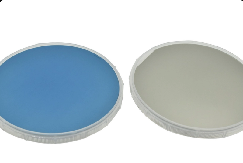
| Surface: as-cut, single side polished, double side polished |
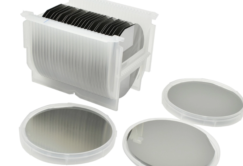
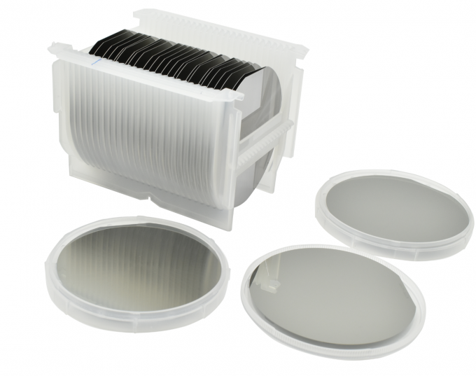
Single Crystal Germanium Wafer Capability
we can offer both electronics grade and IR grade Ge wafer and Ge ingot , please contact us for more Ge product information .
| Conductivity | Dopant | Resistivity ( ohm-cm ) | Wafer Size |
|---|---|---|---|
| NA | Undoped | >= 30 | Up to 4 inch |
| N type | Sb | 0.001 ~ 30 | Up to 4 inch |
| P type | Ga | 0.001 ~ 30 | Up to 4 inch |
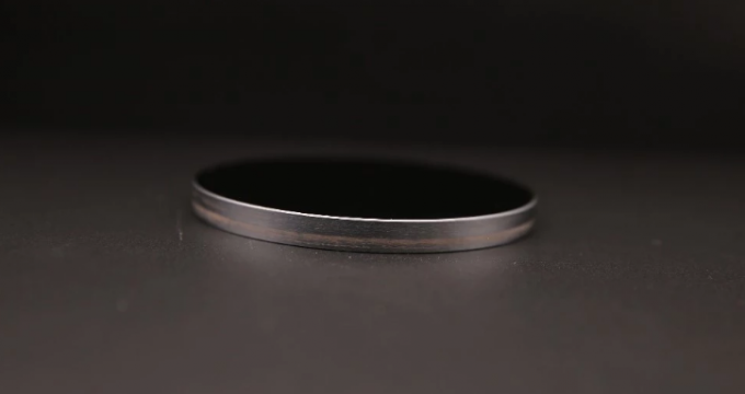
Ge wafer is an elemental and popular semiconductor material , due to its excellent crystallographic properties and unique electric properties , Ge wafer is widly used in Sensor , Solar cell and Infrared optics applications .
We can provide low dislocation and epi ready Ge wafers to meet your unique requirement. Ge wafer is produced as per semiconductor,with a good quality control system , ZMKJ Is dedicated to providing clean and high quality Ge wafer products .
we can offers both electronics grade and IR grade Ge wafer , please contact us for more Ge product information.
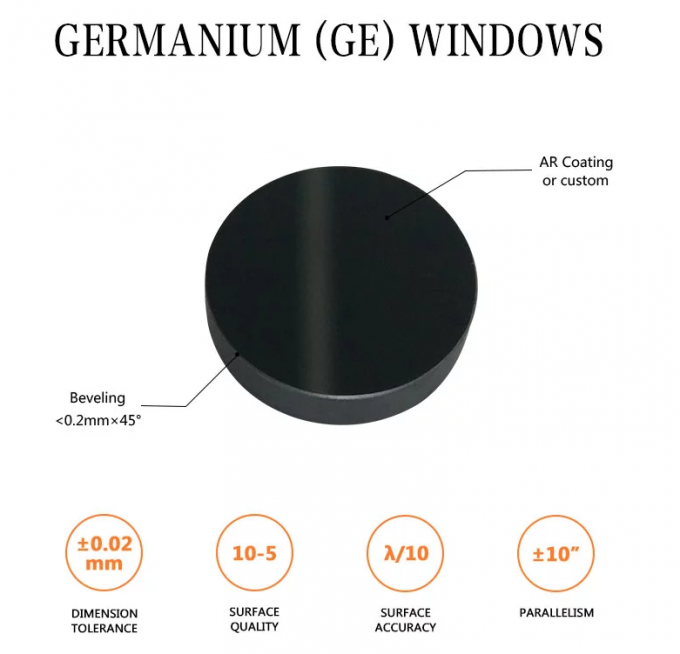
In the range of 2-12 μm, germanium is the most commonly used material for the production of spherical lenses and windows for high efficiency infrared in imaging system. Germanium has a high refractive index (about 4.0 through 2-14μm band), usually do not need to be modified due to its low chromatic aberration in low power imaging systems.

| SL.No | Material Specifications: | |
| 1 | Crystalline Form : | Polycrystalline |
| 2 | Conductivity Type : | n-type |
| 3 | Absorption Coefficient, at 25°C | 0.035cm-1 max @10.6µm |
| 4 | Typical Resistivity : | 3-40 ohm-cm |
| 5 | Density : | 5.3 g/cc |
| 6 | Mohs Hardness : | 6.3 |
| 7 | Oxygen Content : | < 0.03 ppm |
| 8 | Holes and Inclusions: | <0.05 mm |
| 9 | Poisson Ratio : | 0.278 |
| 10 | Youngs Modulus (E) : | 100 Gpa |
| SL.No | Optical Properties: | |
| 1 | dn/dt from 250-350 K : | 4 X 10⁻⁴ K-1 |
| 2 | Transmission at 25°C @10.6 µm wavelength | |
| for uncoated sample of thickness 10mm : | Max. 47% or more | |
| 3 | Refractive Index @ 10.8 µm : | 4.00372471±0.0005 |
| SL.No | Thermal Properties | |
| 1 | Melting Point (K) : | 1210.4 |
| 2 | Heat Capacity @ 300K (J/kg.K): | 322 |
| 3 | Thermal Conductivity @293 K : | 59 Wm-1 K-1 |
| 4 | Coefficient Thermal Expansion @ (20°C) (10-6 K): | 5.8 |
Q: Do you provide samples? Is it free or charged?
· We’d like to supply samples for free if we have it in stock, but we don’t pay freight.
Q: How long is your delivery time?
· Regarding inventory, it is 3 working days;
· For customized one, it’s about 15-25 working days, depended on exact quantity and order date.
Q: Is it possible to customize special lens?
· Yes, to customize special optical element and coating are available here.
Q: How to pay?
· T/T, Alibaba online assurance payment, MoneyGram, West Union, Paypal and so on.
Send Inquiry
