


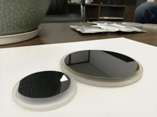
Single Crystal Indium Phosphide Wafers InP wafer
The materials are very suitable for manufacturing high […]
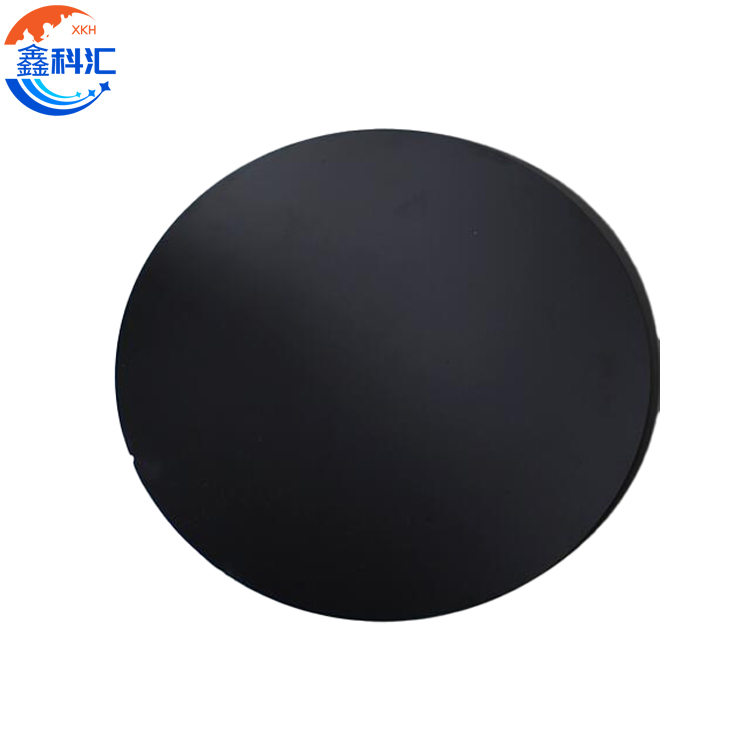
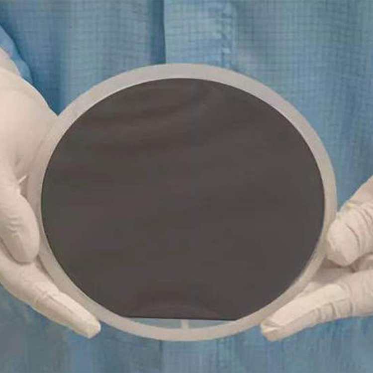
The materials are very suitable for manufacturing high frequency, high speed, high power microwave devices, and integrated circuits. It’s widely used in solid-state lighting, microwave communication, fiber-optic communication, solar cells, guidance/navigation, satellite, and other civil and military fields.Indium Phopshide (InP) is a binary semiconductor composed of Indium (In) and Phosphorus (P), belonging to a group of materials commonly known as III-V Semiconductors.
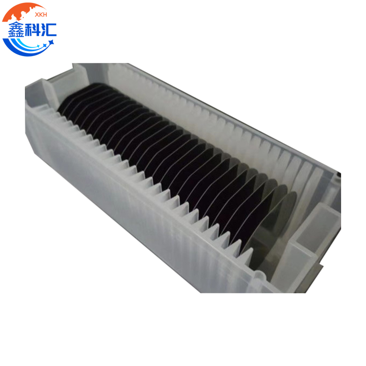
Indium Phosphide Wafer Specifications
| Size | 10 x 10 x 0.35mm, 10 x 5 x 0.35mm, 2” Dia, 3” Dia,4′ Dia (customized sizes are available) |
|---|---|
| Thickness | 0.35 mm, 0.6 mm |
| Polished | SSP or DSP |
| Orientation | <100>, <111> |
| Redirection Precision | ±0.5° |
| Primary Flat Length | 16±2 mm, 22±2 mm, 32.5±2 mm |
| Scondary Flat Length | 8±1 mm, 11±1 mm, 18±1 mm |
| TTV | <10 um, <15 um |
| Bow | <10 um, <15 um |
| Warp | <15 um |

Indium Phosphide Wafer Physical Properties
| Material | InP |
|---|---|
| Growth Method | LEC,VCZ/P-LEC , VGF, VB |
| Lattice (A) | a=5.869 |
| Structure | M3 |
| Melting Point | 1600℃ |
| Density(g/cm3) | 4.79 g/cm3 |
| Doped Material | Undoped S-dopedZn-dopedFe-doped |
| Type | NNPN |
| Carrier Concentration (cm-3) | (0.4-2) x 1016(0.8-3) x 1018 (4-6) x 1018(0.6-2) x 1018107-108 |
| Mobility (cm2v-1s-1) | (3.5-4) x 103(2.2-2.4) x 103 (1.3-1.6) x 10370-90≥2000 |
| EPD (Average) | <5 x 10⁴/cm23 x 104/cm2 2 x 10³/cm22 x 104/cm23 x 104/cm2 |
InP Wafer Supplier—Shanghai Xinkehui New Material Co. Ltd.,
Shanghaixinkehui new material co.,ltd based on JINGJING Tech co.ltd. is a high-tech enterprise specializing in the research and development, production, processing and sales of semiconductor glass wafer , special optical glass and new crystal materials. The company‘s main products include sapphire optical window, sapphire optical components, equipment instrument accessories, mobile phone lens cover, sapphire bearing, special-shaped non-standard parts. The company will adhere to “customer as the center, quality as the foundation”, and strive to build a first-class high-tech enterprise in optoelectronic materials.
FAQ
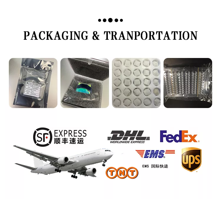
Q: What’s the way of shipping and cost?
(1) We accept DHL, Fedex, TNT, UPS, EMS, SF and etc.
(2) If you have your own express account, it’s great.
Q: How to pay?
(1) T/T, PayPal, West Union, MoneyGram and Assurance payment on Alibaba and etc..
(2) Bank Fee: West Union≤USD1000.00), T/T -: over 1000usd ,please by t/t
For the sake of your financial security,We recommend you to trade through Alibaba SINOSURE.
Q: What’s the deliver time?
(1) For inventory: the delivery time is 5 workdays.
(2) For customized products: the delivery time is 7 to 25 workdays. According to the quantity.
Q: Can I customize the products based on my need?
Yes, we can customize the material, specifications and optical coating for your optical components based on your needs.
Send Inquiry
