

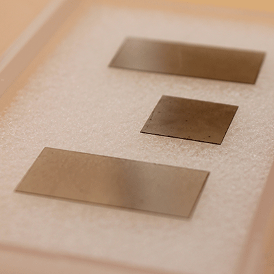
Template On Diamond Wafers Substrate AlN Epitaxial Films
AlN on Diamond template wafers AlN epitaxial films on D […]
AlN on Diamond template wafers AlN epitaxial films on Diamond substrate AlN on Sapphire /AlN-on-SiC/ AlN-ON Silicon
Advantages of AlN Epitaxial Films
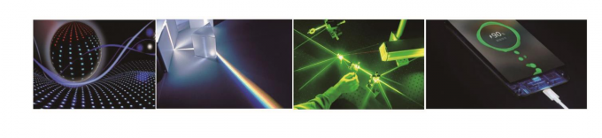
• Direct band gap, band gap width of 6.2eV, is an important deep ultraviolet and ultraviolet luminescent material
• High breakdown electric field strength, high thermal conductivity, high insulation, low dielectric constant, low thermal expansion coefficient, good mechanical performance, corrosion resistance, commonly used in high temperature and high frequency
High power device
• Very good piezoelectric performance (especially along the C-axis), which is one of the best materials for preparing various sensors, drivers and filters
• It has very close lattice constant and thermal expansion coefficient to GaN crystal, and is the preferred substrate material for heteroepitaxial growth of GaN based optoelectronic devices.
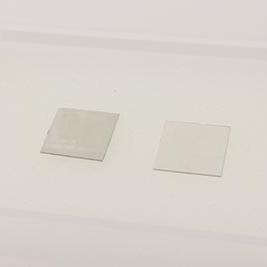
Three Major AlN Products
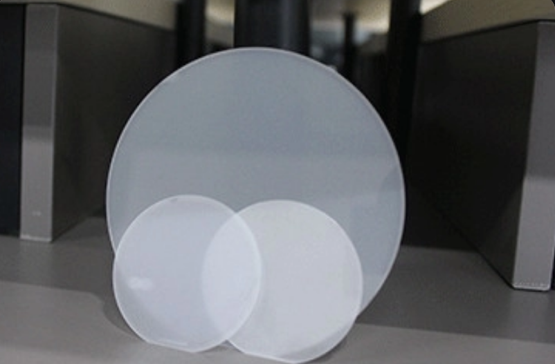
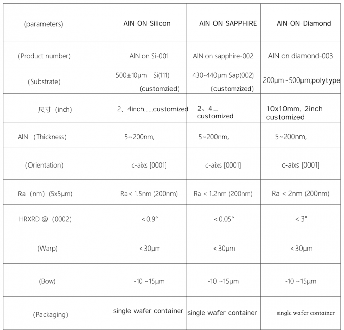
1. AlN-ON-Silicon
High quality aluminum nitride (AlN) thin films were successfully prepared on silicon substrate by composite deposition. The half peak width of the XRD (0002) rocking curve is less than 0.9 °, and the surface roughness of the growth surface is Ra<
1.5nm (aluminum nitride thickness 200nm), high-quality aluminum nitride film helps to realize the preparation of gallium nitride (GaN) in large size, high quality and low cost.
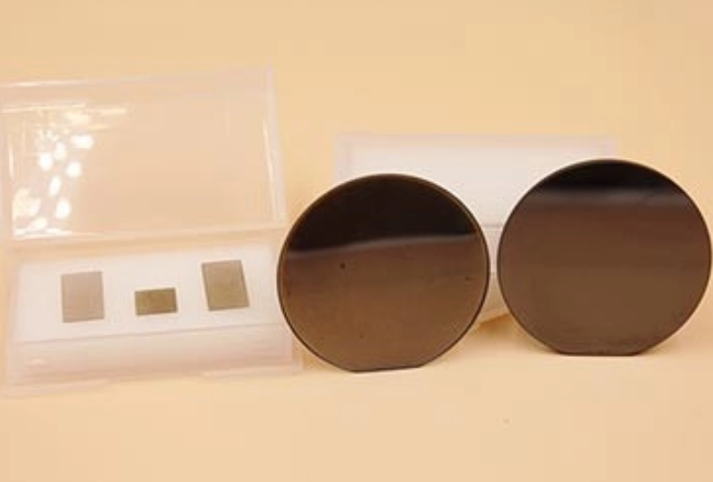
2. Sapphire based AlN-On-Sapphire
High quality AlN on Sapphire (sapphire based aluminum nitride) prepared by composite deposition, half peak width of XRD (0002) swing curve<0.05 °, surface roughness of growth surface
Ra<1.2nm (aluminum nitride thickness is 200nm), which not only realizes effective control of product quality, greatly improves product quality, ensures product stability, but also greatly reduces
The product cost and production cycle are reduced. The customer verification shows that the high-quality AlN on Sapphire of CSMC can greatly improve the yield and stability of UVC LED products
Qualitative, helping to improve product performance.
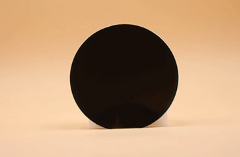
3. Diamond based AlN-On-Diamond
CVMC is the world’s first, and innovatively develops diamond based aluminum nitride. The half peak width of the XRD (0002) swing curve is less than 3 °, and the diamond has ultra-high thermal conductivity (the thermal conductivity at room temperature can
Up to 2000W/m K) The surface roughness of the growth surface Ra < 2nm (the thickness of aluminum nitride is 200nm), helping the new application of aluminum nitride.
Application Advantages of AlN Epitaxial Films
• UVC LED substrate
Driven by the process cost and the requirements of high yield and high uniformity, the substrate of AlGaN based UVC LED chip is of large thickness, large size and suitable slope.Chamfered sapphire substrates are a great choice. The thicker substrate can effectively alleviate the abnormal distortion of epitaxial wafers caused by stress concentration during epitaxy
The uniformity of epitaxial wafers can be improved; Larger substrates can greatly reduce the edge effect and quickly reduce the overall cost of the chip; Suitable chamfer angle can
To improve the surface morphology of the epitaxial layer, or combine with the epitaxial technology to form the Ga rich carrier localization effect in the active region of the quantum well, so as to improve the luminous efficiency.
• Transition layer
Using AlN as buffer layer can significantly improve the epitaxial quality, electrical and optical properties of GaN films. The lattice mismatch between GaN and AIN substrate is 2.4%, the thermal mismatch is almost zero, which can not only avoid the thermal stress caused by high temperature growth, but also greatly improve the production efficiency.
• Other applications
In addition, AlN thin films can be used for piezoelectric thin films of surface acoustic wave devices (SAW), piezoelectric thin films of bulk acoustic wave devices (FBAR), insulating buried layers of SOI materials, and monochromatic cooling
Cathode materials (used for field emission displays and micro vacuum tubes) and piezoelectric materials, high thermal conductivity devices, acousto-optic devices, ultra ultraviolet and X-ray detectors.
Empty collector electrode emission, dielectric material of MIS device, protective layer of magneto-optical recording medium.
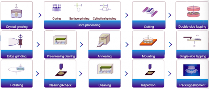
Processing Flow of AlN Epitaxial Films
- Sapphire body
- Slicing
- Edge Chamfering
- Lapping
- Annealing
- Polishing
- Inspection
- Cleaning&Packing
FAQ & CONTACT
Q:What is your minimum order requirement?
A:MOQ:1 piece
Q:How long will it take to execute my order ?
A:After confirming the payment.
Q:Can you give warranty of your products ?
A:We promise the quality, if the quality has any problems, we will produce new produces or return you money.
Q:How to pay?
A:T/T, Paypal, West Union, bank transfer and or Assurance payment on Alibaba and etc.
Q:Can you produce custom optics?
A:Yes, we can produce custom optics
Q:If you have any other questions,please do not hesitate to contact me.
A:Tel+:86-18621835134 Email: gery@xinkehui.cn
Send Inquiry
