

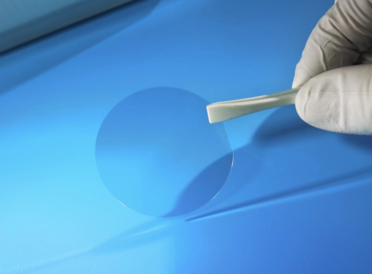
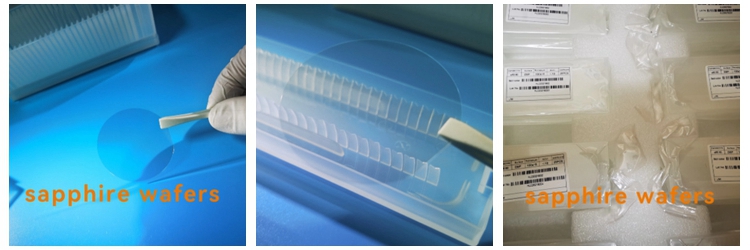
100um Ultra Thin Sapphire Substrate Wafer High Optical Transmittance DSP
The Detail for 2inch C-axis wafers […]
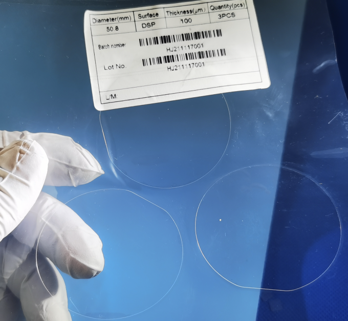
The Detail for 2inch C-axis wafers
Size: 2 inch DSP-0.1-C-Sapphire
Material: KY Sapphire Al2O3 single crystal without bubble;color ;
Orientation:R-cut,R-axis off 0.0+/-0.1°;
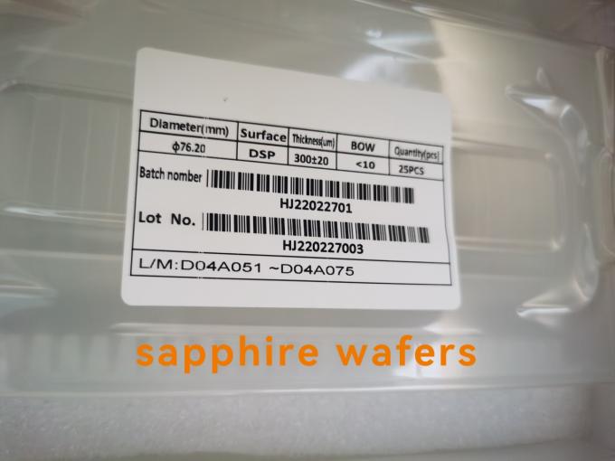
Diameter: 50.8 +/-0.2mm ;
Thickness:100 ± 15 um ;
OF Flat:16.0 +/- 1.0 mm ;
OF orientation: A-axis
Surface: SSP Epi-ready Polished ;
TTV<= 10um ;BOW<= 20um ; Warp<= 20 um ;
Front Surface Roughness (Ra) Ra <= 0.3 nm;
Back Surface Roughness (Ra) Ra = 1.0 +/-0.2um ;
Edge: from 1mm ;
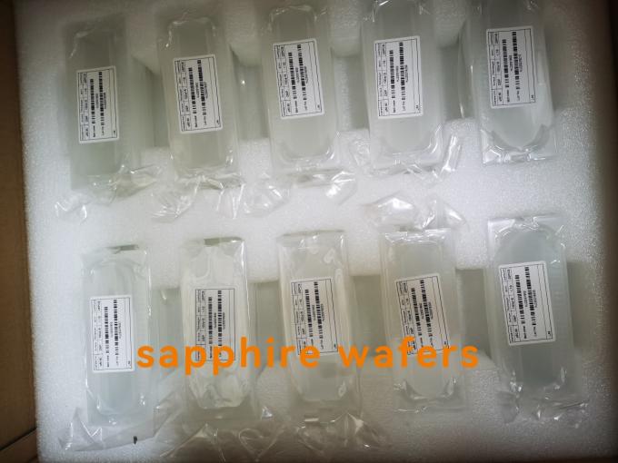
General Other Size Sheet on Stocks
| Standard wafer2 inch C-plane sapphire wafer SSP/DSP0.1mm,0.175mm, 0.2mm; 0.3mm,0.4mm,0.5mm 3 inch C-plane sapphire wafer SSP/DSP0.43mm,0.5mm; 4 inch C-plane sapphire wafer SSP/DSP0.25mm,0.3mm,0.4mm,0.5mm,0.65mm 6 inch C-plane sapphire wafer SSP/DSP1.0mm,1.3mm, 0.8mm | Special Orientation A-plane (1120) sapphire wafer R-plane (1102) sapphire wafer M-plane (1010) sapphire waferAll on stocks C-axis with a 0.5°~ 10° offcut, toward A-axis or M-axis Other customized orientation |
| Customized Size 10x10x0.5mm sapphire wafer 20x20x0.5mm sapphire wafer Ultra thin (100um) 2inch sapphire wafer 8 inch sapphire wafer | Patterned Sapphire Substrate (PSS) 2 inch C-plane PSS 4 inch C-plane PSS |
FEATURES OF SINGLE CRYSTAL SAPPHIRE
1. Sapphire has a high optical transmittance, so it is widely used as microelectronic tube dielectric material, ultrasonic conduction element, waveguide laser cavity, and other optical elements, as window materials for infrared military devices, space vehicles, high-intensity lasers and optical communications.
2. Sapphire has high rigidity, high strength, high working temperature, abrasion resistance, corrosion resistance characteristics, so sapphire substrate is often used in harsh environments, such as boiler water gauge (high-temperature resistance), commodity bar code scanner, bearing, and other precision manufacturing (wear resistance), coal, gas, well detection sensors and detector windows (anti-corrosion).
3. Sapphire has the characteristics of electrical insulation, transparency, good thermal conductivity, and high rigidity, so it can be used as the substrate material of integrated circuits, such as LED and microelectronic circuits, ultra-high-speed integrated circuit.
1. Q: Where is your company located? How can I visit there?
A: Our factory is located in Wuxi City, Jiangsu Province, China.
2. Q: Can I get sample and how long will it take?
A:Yes. We can supply sample. And you need to pay for the sample and courier. About 7days after receiving the payment, we will send it out.
3. Q: What’s the MOQ?
A: Our MOQ is 25 pieace for this size.
4. Q: Can I have my own customized product?
A: Yes. Your customized requirements for logo, design, package, carton mark, your language manual etc. are very welcome.
5. Q: Can I mix different models in one container?
A: Yes. Different models can be mixed in one container.
6. Q: What is the payment terms?
A:100% T/T
If you have another question, pls feel free to contact us by E-mail or Tel.
Send Inquiry
