

VGF 6 Inch N Type GaAs Semiconductor Substrate For Epitaxial Growth
VGF 2inch 4inch 6inch n-type prime grade GaAs wafer for […]
VGF 2inch 4inch 6inch n-type prime grade GaAs wafer for epitaxial growth
GaAs wafer (Gallium Arsenide) is an advantageous alternative to silicon that has been evolving in the semiconductor industry. Less power consumption and more efficiency offered by this GaAs wafers are attracting the market players to adopt these wafers, thereby increasing the demand for GaAs wafer. Generally, this wafer is used to manufacture semiconductors, light emitting diodes, thermometers, electronic circuits, and barometers, besides finding application in the manufacturing of low melting alloys. As the semiconductor and electronic circuit industries continue to touch new peaks, the GaAs market is booming. Gallium arsenide of GaAs wafer has the power of generating laser light from electricity. Especially polycrystalline and single crystal are the two major type of GaAs wafers, which are utilized in the production of both the microelectronics and optoelectronics to create LD, LED, and microwave circuits. Therefore, the extensive range of GaAs applications, particularly in optoelectronics and microelectronics industry is creating a demand influx in the GaAs Wafer Market. Previously, the optoelectronic devices were mainly used on a broad range in short-range optical communications and computer peripherals. But now, they are in demand for some emerging applications such as LiDAR, augmented reality, and face recognition. LEC and VGF are two popular methods which are improving the production of GaAs wafer with high uniformity of electrical properties and excellent surface quality. Electron mobility, single junction band-gap, higher efficiency, heat and moisture resistance, and superior flexibility are the five distinct advantages of GaAs, which are improving the acceptance of GaAs wafers in the semiconductor industry.
| GaAs (Gallium Arsenide) for LED Applications | ||
| Item | Specifications | Remarks |
| Conduction Type | SC/n-type | |
| Growth Method | VGF | |
| Dopant | Silicon | |
| Wafer Diamter | 2, 3 & 4 inch | Ingot or as-cut available |
| Crystal Orientation | (100)2°/6°/15° off (110) | Other misorientation available |
| OF | EJ or US | |
| Carrier Concentration | (0.4~2.5)E18/cm3 | |
| Resistivity at RT | (1.5~9)E-3 Ohm.cm | |
| Mobility | 1500~3000 cm2/V.sec | |
| Etch Pit Density | <500/cm2 | |
| Laser Marking | upon request | |
| Surface Finish | P/E or P/P | |
| Thickness | 220~350um | |
| Epitaxy Ready | Yes | |
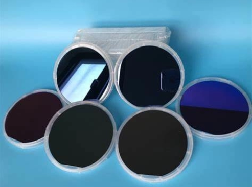
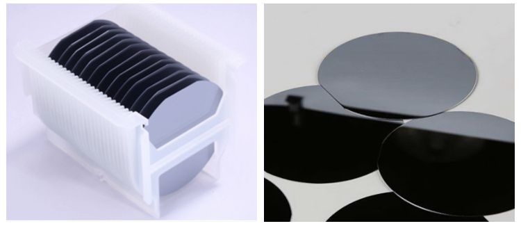
| Package | Single wafer container or cassette |
| GaAs (Gallium Arsenide) ,Semi-insulating for Microelectronics Applications | ||
| Item | Specifications | Remarks |
| Conduction Type | Insulating | |
| Growth Method | VGF | |
| Dopant | Undoped | |
| Wafer Diamter | 2, 3, 4 & 6 inch | Ingot available |
| Crystal Orientation | (100)+/- 0.5° | |
| OF | EJ, US or notch | |
| Carrier Concentration | n/a | |
| Resistivity at RT | >1E7 Ohm.cm | |
| Mobility | >5000 cm2/V.sec | |
| Etch Pit Density | <8000 /cm2 | |
| Laser Marking | upon request | |
| Surface Finish | P/P | |
| Thickness | 350~675um | |
| Epitaxy Ready | Yes | |
| Package | Single wafer container or cassette |
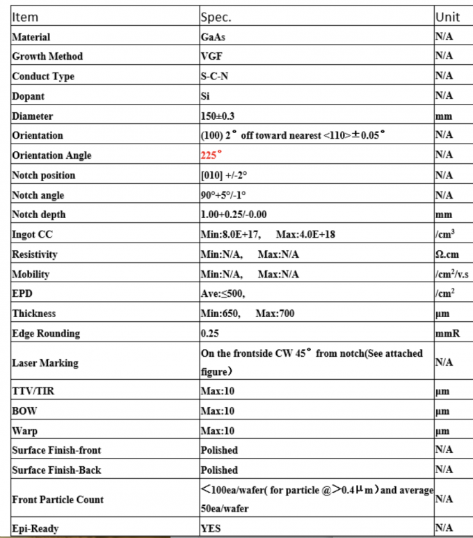
| No. | Item | Standard Specification | ||||
| 1 | Size | 2″ | 3″ | 4″ | 6″ | |
| 2 | Diameter | mm | 50.8±0.2 | 76.2±0.2 | 100±0.2 | 150±0.5 |
| 3 | Growth Method | VGF | ||||
| 4 | Doped | Un-doped, or Si-doped, or Zn-doped | ||||
| 5 | Conductor Type | N/A, or SC/N, or SC/P | ||||
| 6 | Thickness | μm | (220-350)±20 or (350-675)±25 | |||
| 7 | Crystal Orientation | <100>±0.5 or 2 off | ||||
| OF/IF Orientation Option | EJ, US or Notch | |||||
| Orientation Flat (OF) | mm | 16±1 | 22±1 | 32±1 | – | |
| Identification Flat (IF) | mm | 8±1 | 11±1 | 18±1 | – | |
| 8 | Resistivity | (Not for Mechanical Grade) | Ω.cm | (1-30)´107, or (0.8-9)´10-3, or 1´10-2-10-3 | ||
| Mobility | cm2/v.s | ≥ 5,000, or 1,500-3,000 | ||||
| Carrier Concentration | cm-3 | (0.3-1.0)x1018, or (0.4-4.0)x1018, or As SEMI | ||||
| 9 | TTV | μm | ≤10 | |||
| Bow | μm | ≤10 | ||||
| Warp | μm | ≤10 | ||||
| EPD | cm-2 | ≤ 8,000 or ≤ 5,000 | ||||
| Front/Back Surface | P/E, P/P | |||||
| Edge Profile | As SEMI | |||||
| Particle Count | <50 (size>0.3 μm,count/wafer), or AS SEMI | |||||
| 10 | Laser Mark | Back side or upon request | ||||
| 11 | Packaging | Single wafer container or cassette |
What is GaAs substrate?
Wafer Technology offers single crystal Gallium Arsenide grown at low pressure from high purity polycrystalline Gallium Arsenide in a vertical temperature gradient (VGF-Vertical Gradient Freeze).
What type of semiconductor is GaAs?
What type of semiconductor is GaAs?
type III/V semiconductor
Gallium arsenide is a type III/V semiconductor, with high electron mobility and a high saturated electron velocity compared to silicon, enabling transistors made of gallium arsenide to function at frequencies over 250 GHz
How is GaAs formed?
How is GaAs formed?
GaAs crystals can be created through three different methods. One of the more common methods is the vertical gradient freeze process, which involves growing crystals and slicing them, followed by edge rounding and polishing them into wafers. Another method is the Bridgman-Stockbarger technique.
Send Inquiry
