

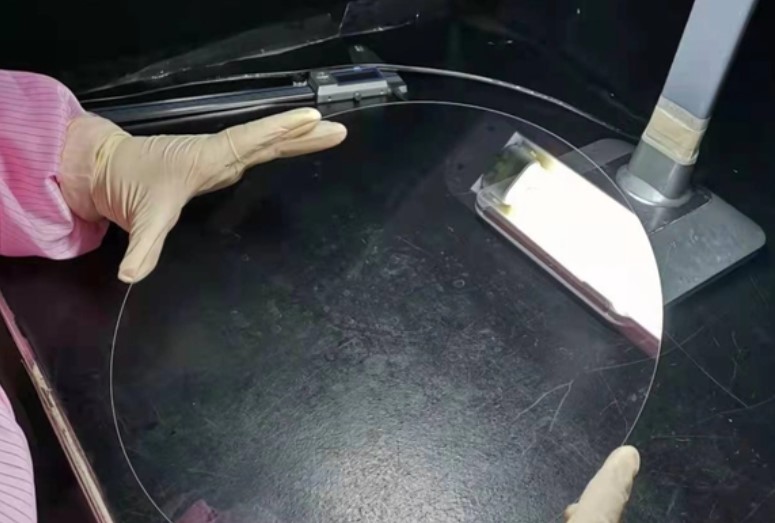
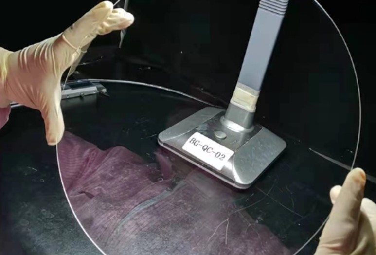
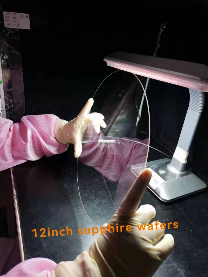
12 Inch Sapphire Substrate Dia 300mm C Plane Quartz Wafers BF33
The Detail for 12inch C-axis wafers   […]
The Detail for 12inch C-axis wafers
Size: 12inch DSP-1.0-C-Sapphire
Material: KY Sapphire Al2O3 single crystal without bubble;color ;
Orientation:C-cut,+/-0.3°;
Diameter: 300 +/-0.2mm ;
Thickness:1000 ± 25 um ;
OF Flat: Notch at A-axis;
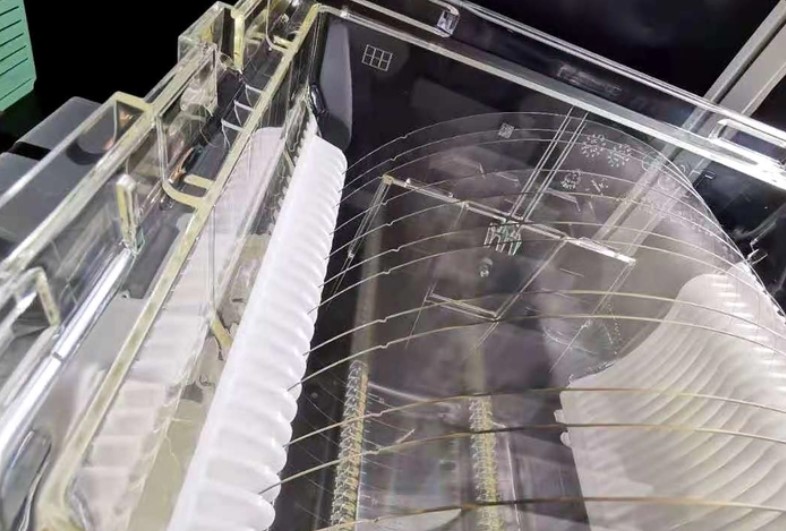
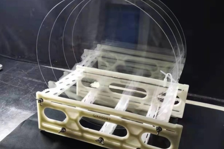
Surface: DSP Epi-ready Polished ;
TTV<= 20um ;BOW<= 30um ; Warp<= 45 um ;
Front Surface Roughness (Ra) Ra <= 0.3 nm;
Back Surface Roughness (Ra) Ra = 0.3 +/-0.2um ;
Edge: from 1mm ;
FEATURES OF SINGLE CRYSTAL SAPPHIRE
1. Sapphire has a high optical transmittance, so it is widely used as microelectronic tube dielectric material, ultrasonic conduction element, waveguide laser cavity, and other optical elements, as window materials for infrared military devices, space vehicles, high-intensity lasers and optical communications.
2. Sapphire has high rigidity, high strength, high working temperature, abrasion resistance, corrosion resistance characteristics, so sapphire substrate is often used in harsh environments, such as boiler water gauge (high-temperature resistance), commodity bar code scanner, bearing, and other precision manufacturing (wear resistance), coal, gas, well detection sensors and detector windows (anti-corrosion).
3. Sapphire has the characteristics of electrical insulation, transparency, good thermal conductivity, and high rigidity, so it can be used as the substrate material of integrated circuits, such as LED and microelectronic circuits, ultra-high-speed integrated circuit.
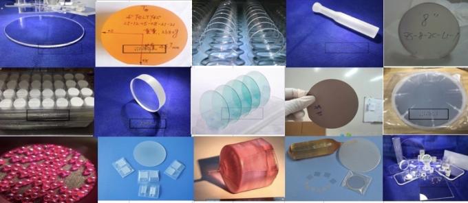
General Other Size Sheet on Stocks
| Standard wafer 2 inch C-plane sapphire wafer SSP/DSP0.1mm,0.175mm, 0.2mm; 0.3mm,0.4mm,0.5mm 3 inch C-plane sapphire wafer SSP/DSP0.43mm,0.5mm; 4 inch C-plane sapphire wafer SSP/DSP0.25mm,0.3mm,0.4mm,0.5mm,0.65mm 6 inch C-plane sapphire wafer SSP/DSP1.0mm,1.3mm, 0.8mm | Special Orientation A-plane (1120) sapphire wafer R-plane (1102) sapphire wafer M-plane (1010) sapphire waferAll on stocks C-axis with a 0.5°~ 10° offcut, toward A-axis or M-axis Other customized orientation |
| Customized Size 10x10x0.5mm sapphire wafer 20x20x0.5mm sapphire wafer Ultra thin (100um) 2inch sapphire wafer 8 inch sapphire wafer | Patterned Sapphire Substrate (PSS) 2 inch C-plane PSS 4 inch C-plane PSS |
EXCELLENT SAPPHIRE WAFERS
- 99.999 % high purity single crystal Al2O3 material.
- Special CMP (Chemical Mechanical Polishing) technology to ensure the performance of Al2O3 substrate at a low cost.
- Excellent surface quality in all orientations (less than 0.2 nm for C-plane, less than 0.5 nm for A-plane, M-plane, R-plane, N-plane, V-plane, 10-14, etc.)
- Cleaned in class 100 cleanroom by ultrapure water with quality above 18MΩ *cm.
- 25 pcs a pack or single pack is available to maximize customer flexibility in their research.
- Traceable product serial number.
- Compact carton packaging for safer shipping and cost-saving.
- Standard wafers are Generally in stock to ensure a quick delivery.
Sapphire application
- 1. Semiconductor LED industry (MOCVD epitaxial GaN substrate)
- In general, C-plane sapphire is needed in this area. R-plane or M-plane mainly used to grow non-polar/semi-polar plane epitaxial layers to improve the luminescence efficiency.
- 2. The growth of III-V or II-VI compound semiconductors.
- 3. Microelectronic IC applications especially Very High-Speed Integrated Circuit, SOS
- Generally, it is a silicon heteroepitaxial deposition on R-plane sapphire.
- 4. Hybrid microelectronics
- Hybrid microelectronics products are mainly HIC and MCM. It has high requirements on the substrate, while sapphire substrates’ characteristics such as stable dielectric constant and low dielectric loss make sapphire wafer the most commonly used substrate for HIC and the main substrate for MCM. Generally, the A-plane sapphire wafer is needed.
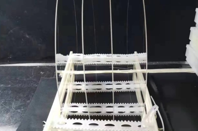
Packing & Delivery
Packing Details : Packing, BOX,CARTONS
Delivery Details : 3-7 working days after order of Solid bicycle tire tubesrecieving your pament will be send out.
FAQ
1. Q: Where is your company located? How can I visit there?
A: Our factory is located in Wuxi City, Jiangsu Province, China.
2. Q: Can I get sample and how long will it take?
A:Yes. We can supply sample. And you need to pay for the sample and courier. About 7days after receiving the payment, we will send it out.
3. Q: What’s the MOQ?
A: Our MOQ is 25 pieace for this size.
4. Q: Can I have my own customized product?
A: Yes. Your customized requirements for logo, design, package, carton mark, your language manual etc. are very welcome.
5. Q: Can I mix different models in one container?
A: Yes. Different models can be mixed in one container.
6. Q: What is the payment terms?
A:100% T/T
Send Inquiry
