


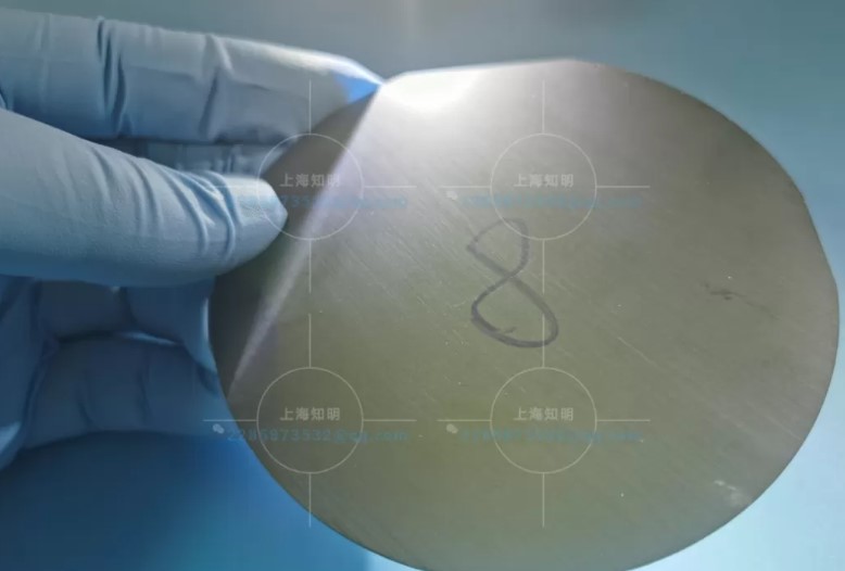
1.5mm Thickness 4h-N 4H-SEMI SIC Silicon Carbide Wafer For Epitaxial
Silicon carbide (SiC), also known as carborundum, is a […]
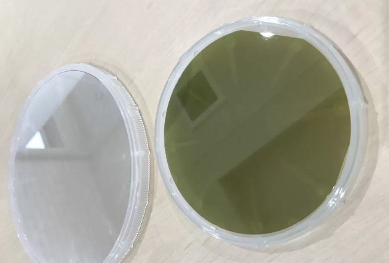
Silicon carbide (SiC), also known as carborundum, is a semiconductor containing silicon and carbon with chemical formula SiC. SiC is used in semiconductor electronics devices that operate at high temperatures or high voltages, or both.SiC is also one of the important LED components, it is a popular substrate for growing GaN devices, and it also serves as a heat spreader in high-power LEDs.
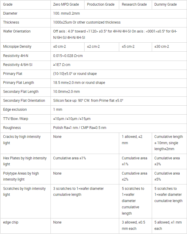
| Property | 4H-SiC, Single Crystal | 6H-SiC, Single Crystal |
| Lattice Parameters | a=3.076 Å c=10.053 Å | a=3.073 Å c=15.117 Å |
| Stacking Sequence | ABCB | ABCACB |
| Mohs Hardness | ≈9.2 | ≈9.2 |
| Density | 3.21 g/cm3 | 3.21 g/cm3 |
| Therm. Expansion Coefficient | 4-5×10⁻⁶/K | 4-5×10⁻⁶/K |
| Refraction Index @750nm | no = 2.61 ne = 2.66 | no = 2.60 ne = 2.65 |
| Dielectric Constant | c~9.66 | c~9.66 |
| Thermal Conductivity (N-type, 0.02 ohm.cm) | a~4.2 W/cm·K@298K c~3.7 W/cm·K@298K | |
| Thermal Conductivity (Semi-insulating) | a~4.9 W/cm·K@298K c~3.9 W/cm·K@298K | a~4.6 W/cm·K@298K c~3.2 W/cm·K@298K |
| Band-gap | 3.23 eV | 3.02 eV |
| Break-Down Electrical Field | 3-5×10⁶V/cm | 3-5×10⁶V/cm |
| Saturation Drift Velocity | 2.0×10⁵m/s | 2.0×10⁵m/s |
CATALOGUE COMMON SIZE In OUR INVENTORY LIST
| 4H-N Type / High Purity SiC wafer/ingots 2 inch 4H N-Type SiC wafer/ingots 3 inch 4H N-Type SiC wafer 4 inch 4H N-Type SiC wafer/ingots 6 inch 4H N-Type SiC wafer/ingots | 4H Semi-insulating / High Purity SiC wafer 2 inch 4H Semi-insulating SiC wafer 3 inch 4H Semi-insulating SiC wafer 4 inch 4H Semi-insulating SiC wafer 6 inch 4H Semi-insulating SiC wafer |
| 6H N-Type SiC wafer 2 inch 6H N-Type SiC wafer/ingot | Customzied size for 2-6inch |
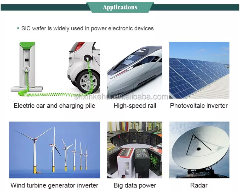
Application areas
- 1 high frequency and high power electronic devices Schottky diodes, JFET, BJT, PiN,
- diodes, IGBT, MOSFET
- 2 optoelectronic devices: mainly used in GaN/SiC blue LED substrate material (GaN/SiC) LED
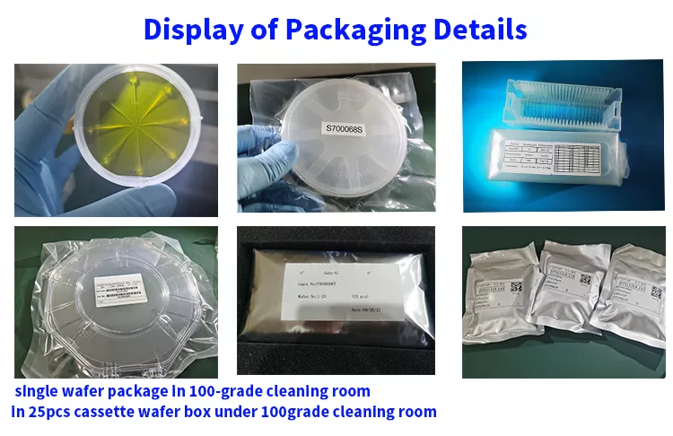
>Packaging – Logistcs
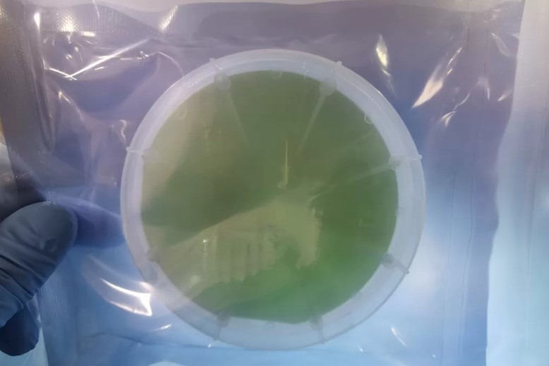
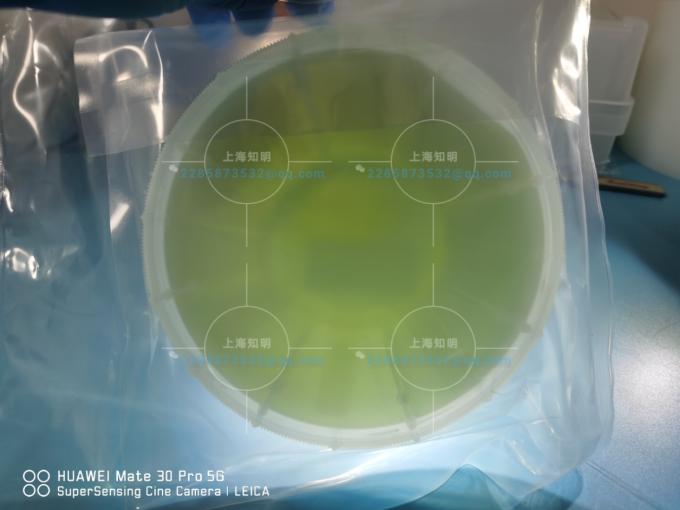
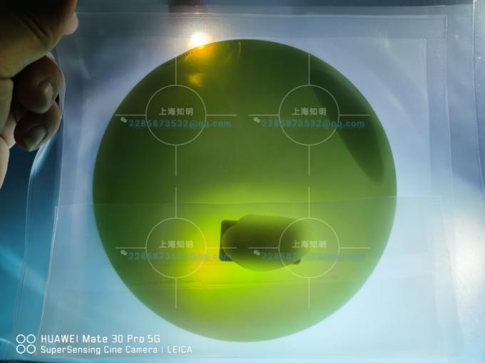
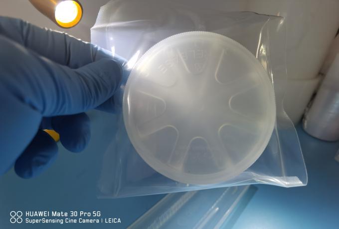
we concerns each details of the package , cleaning, anti-static , shock treatment .
According to the quantity and shape of the product , we will take a different packaging process! Almost by single wafer cassettes or 25pcs cassette in 100 grade cleaning room.
FAQ
Q1. Are you a factory?
A1. Yes, we are a professional manufacturer of optical components, we have more than 8years experience in wafers and optical lens process.
Q2. What is the MOQ of your products?
A2. No MOQ for customer if our product is in stock, or 1-10pcs.
Q3:Can I custom the products based on my requirement?
A3.Yes, we can custom the material, specifications and optical coating for your optical components as your requirement.
Q4. How can I get sample from you?
A4. Just send us your requirements, then we will sendsamples accordingly.
Q5. How many days will samples be finished? How about mass products?
A5. Generally, we need 1~2 weeks to finish the sample production. As for the mass products, it depends on your order quantity.
Q6. What’s the delivery time?
A6.
(1)For inventory: the delivery time is 1-3 working days.
(2) For customized products: the delivery time is 7 to 25 working days.
According to the quantity.
Q7. How do you control the quality?
A7. More than four times quality inspect during production process,we can provide the Quality test report.
Q8. How about your optical lens production ability per Month?
A8. About 1,000pcs/Month.According to the detail requirement.
Send Inquiry
