

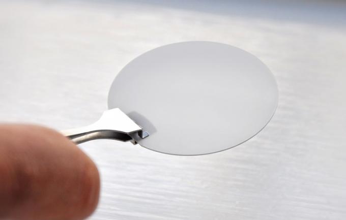
2 4 Inch 4-5 Um III Gallium Nitride Wafer 0.43 Mm Sapphire Sic Substrates
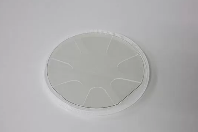
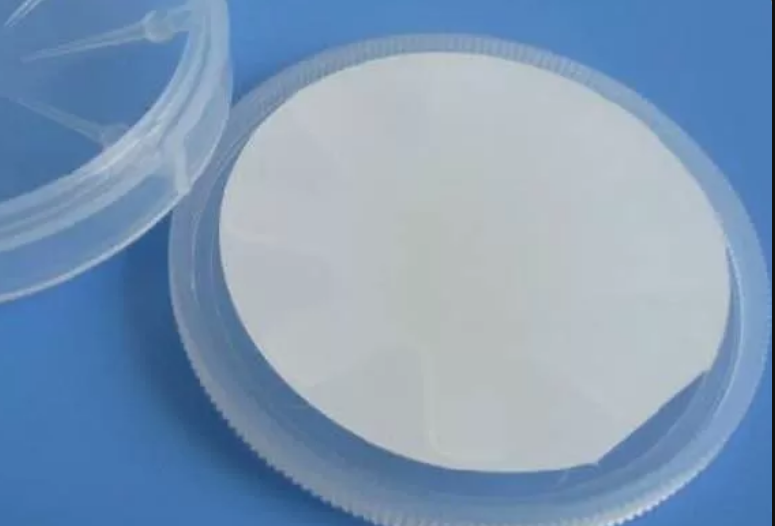
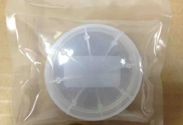
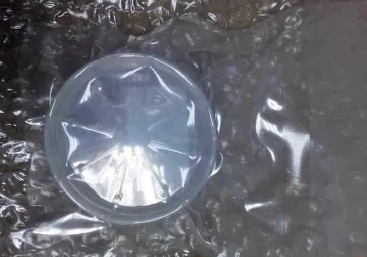
2inch GaN substrates template,GaN wafer for LeD,semicon […]
2inch GaN substrates template,GaN wafer for LeD,semiconducting Gallium Nitride Wafer for ld,GaN template, mocvd GaN Wafer,Free-standing GaN Substrates by Customized size,small size GaN wafer for LED, mocvd Gallium Nitride wafer 10x10mm,5x5mm, 10x5mm GaN wafer,Non-Polar Freestanding GaN Substrates(a-plane and m-plane)
GaN Wafer Characteristic—-III-Nitride(GaN,AlN,InN)
Gallium Nitride is one kind of wide-gap compound semiconductors. Gallium Nitride (GaN) substrate is
a high-quality single-crystal substrate. It is made with original HVPE method and wafer processing technology, which has been originally developed for 10+years in China. The features are high crystalline, good uniformity, and superior surface quality. GaN substrates are used for many kinds of applications, for white LED and LD(violet, blue and green) Furthermore, development has progressed for power and high frequency electronic device applications.
Forbidden band width (light emitting and absorption) cover the ultraviolet, visible light and infrared.
| n-type | p-type | Semi-insulating | |
|---|---|---|---|
| n [cm-3] | up to 1019 | – | – |
| p [cm-3] | – | up to 1018 | – |
| p [cm-3] | 10-3-10-2 | 102-103 | 109-1012 |
| μ [cm2/Vs] | up to 150 | – | – |
| Total Thickness Variation (TTV)/µm | <40 | <40 | <40 |
| Bow/µm | <10 | <10 | <10 |
| FWHM [arcsec] of X-ray rocking curve, epi-ready surface, at 100 μm x 100 μm slit | <20 | ||
| Dislocation Density [cm-2] | <105 | ||
| Misorientation/deg | On demand | ||
| Surface Finish | As cut / ground Roughly polished Optically polished (RMS < 3 nm) Epi-ready (RMS < 0.5 nm) |
Advantages of this Specification
| Smaller Curvature | Fewer Dislocations | More Electrical Carriers | |
| Lasers | Higher Yields | Lower threshold voltage | Higher power |
| LEDs | Better efficiency (IQE) | ||
| Transistors | Lower leakage current | Higher po |
Application of GaN Wafer
GaN can be used in many areas such as LED display, High-energy Detection and Imaging, Laser Projection Display, Power Device, etc.
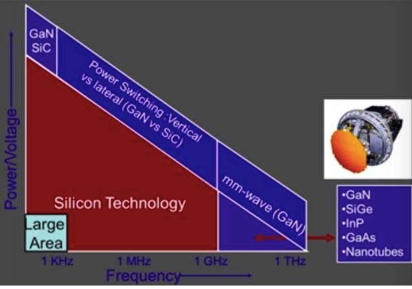
- High- Frequency Microwave Devices High-energy Detection and imagine
- New energy solor hydrogen technology Environment Detection and biological medicine
- Light source terahertz band
- Laser Projection Display, Power Device, etc. Date storage
- Energy-efficient lighting Full color fla display
- Laser Projecttions High- Efficiency Electronic devices
-FAQ –
Q: What’s the MOQ?
(1) For inventory, the MOQ is 2pcs.
(2) For customized products, the MOQ is 5pcs-10pcs.
It depends on quantity and technics.
Q: Do you have inspection report for material?
We can supply ROHS report and reach reports for our products.
Q: What you can supply logistics and cost?
(1) We accept DHL, Fedex, TNT, UPS, EMS, SF and etc.
(2) If you have your own express number, it’s great.
If not, we could assist you to deliver. Freight=USD25.0(the first weight) + USD12.0/kg
Q: What’s the delivery time?
(1) For the standard products such as 2inch 0.33mm wafer.
For inventory: the delivery is 5 workdays after order.
For customized products: the delivery is 2 or 4 workweeks after order.
Q: How to pay?
100%T/T, Paypal, West Union, MoneyGram, Secure payment and Trade Assurance.
Send Inquiry
