

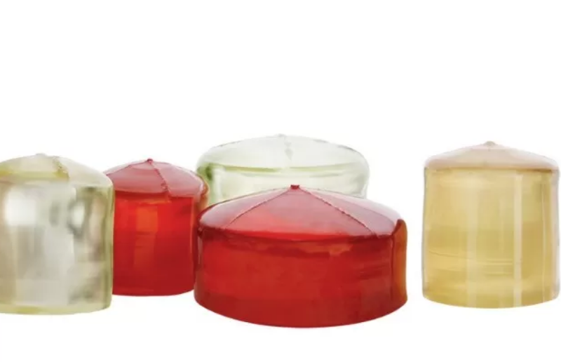
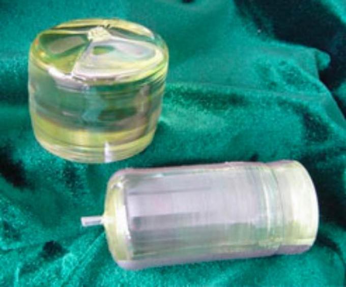
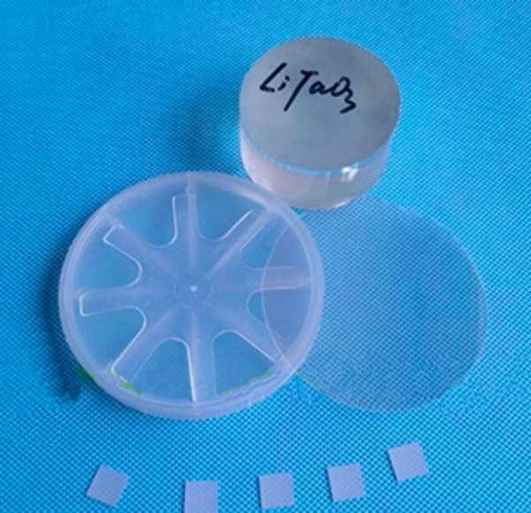
2-6 Inch Semiconductor Substrate LiNbO3 Single Crystal Substrate Wafer
4 inch diameter 100 mm Lithium niobate LiNbO3 substrate […]
4 inch diameter 100 mm Lithium niobate LiNbO3 substrate wafer, LN wafer for saw and optical,SAW Grade LiNbO3 Crystal ingot
Physical and Optical Properties of LiNbO3 Single Crystal Substrate Wafer
| Crystal Structure | Trigonal, space group R3c |
| Cell Parameters | a=0.515,c=13.863,Z=6 |
| Melting Point | 1255 +/-5℃ |
| Curie Point | 1140 +/-5℃ |
| Mohs Hardness | 5 |
| Density | 4.64 g/cm 3 |
| Absorption Coefficient | ~ 0.1%/cm @ 1064 nm |
| Solubility | insoluble in H2O |
| Relative Dielectric Constant | εT11/ε0: 85 εT33/ε0:29.5 |
| Thermal Expansion | ||a, 2.0 x 10 -6/K @ 25℃ |
| Coefficients at 25℃ | ||c, 2.2 x 10 -6/K @ 25℃ |
| Thermal Conductivity | 38 W /m /K @ 25℃ |
| Transparency Range | 420 – 5200 nm |
| Refractive Indices | n e = 2.146, n o = 2.220 @ 1300 nm n e = 2.156, n o = 2.322 @ 1064 nm n e = 2.203, n o = 2.286 @ 633 m |
| Optical Homogeneity | ~ 5 x 10 -5 /cm |
| Sellmeier Equations ( l in mm) | n o 2 (l ) = 4.9048+0.11768/(l2- 0.04750) – 0.027169l2 n e 2 ( l) = 4.5820+0.099169/( l2 – 0.04443) – 0.021950 l2 |
LiNbO3 Single Crystal Substrate Wafer Introduction
Lithium niobate (LiNbO3) is a ferroelectric material suitable for a variety of applications. Its versatility
is made possible by the excellent electro-optic, nonlinear, and piezoelectric properties of the intrinsic material.
It is one of the most thoroughly characterized electro-optic materials, and crystal growing techniques consistently produce large crystals of high perfection.
2-6 Inch Semiconductor Substrate LiNbO3 Single Crystal Substrate Wafer
LiNbO3 Single Crystal Substrate Wafer Application
- Frequency doubling for wavelengths >1μm and optical parametric oscillators (OPOs) pumped at 1064 nm as well as quasi-phase-matched (QPM) devices;
- Pockel cells, Q-switches, and phase modulators;
- Waveguide substrates, surface acoustic wave (SAW) wafers.
| Orientation | 36°Y-cut±0.2° | 41°Y-cut±0.2° | X-cut±0.2° |
| Diameter | 100±0.3mm | ||
| 1st OF Flat | 32±2mm, perpendicular to X-axis±0.2° | 32±2mm,perpendicular to 112°Y±0.2° | |
| 2st OF Flat | 10±2mm CW270°from 1st OF | 10±2mm CW315°from 1st OF | 10±2mm CW315° Or 270°from 1st OF |
| Thickness | 200~250±25um,300-350±25um,500±25um | ||
| Front surface | “+”,Ra<1nm, | ||
| Back surface | GC#1000, GC#2000 Lapped | ||
| LTV | <1um,at5x5mm zone | ||
| BOW | ≤25um |
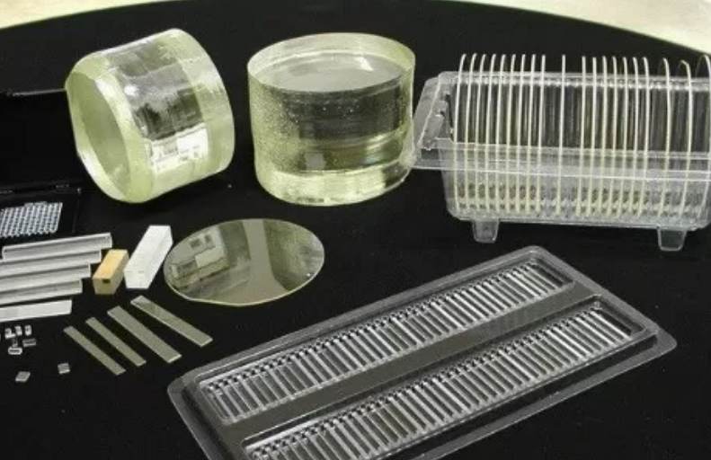
optical Crystal LiNbO3 crystals
| Specification | Conventional | High Precision |
| Materials | LiNbO3(LN) | LiNbO3(LN) |
| Orientation | X-112°Y,36°Y,42°Y±0.5° | X-112°Y,36°Y,42°Y±0.5° |
| Parallel | 30″ | 10” |
| Perpendicular | 10′ | 5′ |
| surface Quality | 40/20 | 20/10 |
| Wavefront Distortion | λ/4@632nm | λ/8@632nm |
| Surface Flatness | λ/4@632nm | λ/8@632nm |
| Clear Aperture | >90% | >90% |
| Chamfer | <0.2×45° | <0.2×45° |
| Thickness/Diameter Tolerance | ±0.1 mm | ±0.1 mm |
| Maximum dimensions | dia150×50mm | dia150×50mm |
FAQ
Q1. Is your company a factory or trade company?
We have a factory and we also do export by our trading company. We are the Sapphire substrates manufactuer.
Q3. How about Pay term & delivery?
T/T,50%deposit and delivery by FOB
Q4. Do you have any stock of wafer or ingots?
We process many size wafer and lens according to customer requirement. So we have few size in stock if it’s commen specifications.
Q5. How long will take to get the products?
Generally it will take 2~4 weeks to process before delivery.
Send Inquiry
