

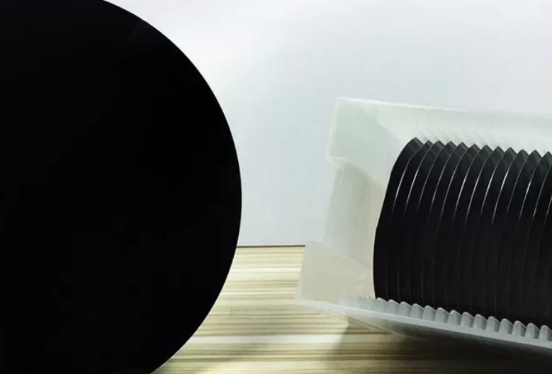
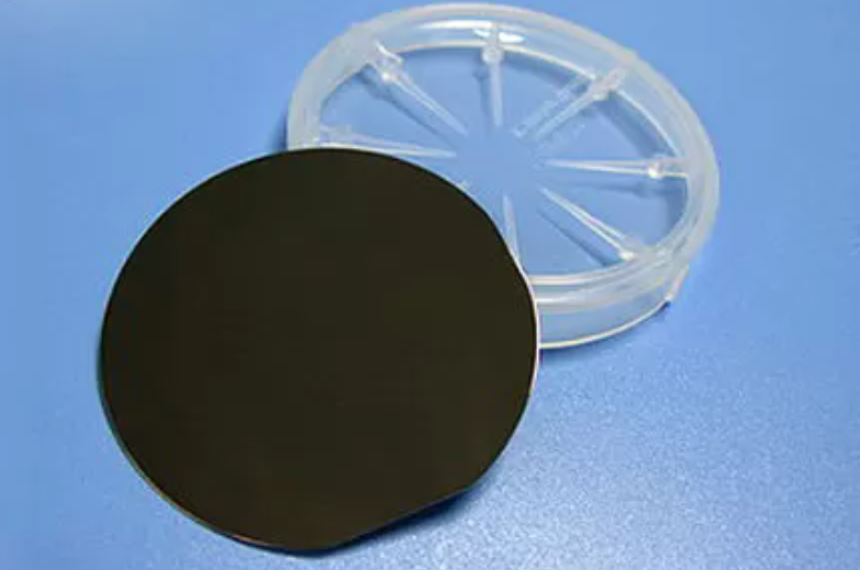
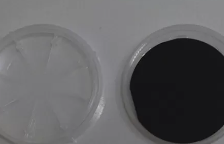
Industrial Semiconductor Substrate S Fe Zn Doped InP Indium Phosphide Single Crystal Wafer
Indium phosphide (InP) is an important compound semicon […]
Indium phosphide (InP) is an important compound semiconductor material with the advantages of high electronic limit drift speed, good radiation resistance and good thermal conductivity. Suitable for manufacturing high frequency, high speed, high power microwave devices and integrated circuits. It is widely used in solid-state lighting, microwave communication, fiber-optic communication, solar cells, guidance/navigation, satellite and other fields of civil and military applications.
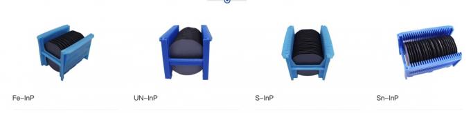
Indium Phosphide which are grown by LEC(Liquid Encapsulated Czochralski) or VGF(Vertical Gradient Freeze) as epi-ready or mechanical grade with n type, p type or semi-insulating in different orientation(111)or(100).
Indium phosphide (InP) is a binary semiconductor composed of indium and phosphorus. It has a face-centered cubic (“zinc blende”) crystal structure, identical to that of GaAs and most of the III-V semiconductors.Indium phosphide can be prepared from the reaction of white phosphorus and indium iodide[clarification needed] at 400 °C.,[5] also by direct combination of the purified elements at high temperature and pressure, or by thermal decomposition of a mixture of a trialkyl indium compound and phosphide. InP is used in high-power and high-frequency electronics[citation needed] because of its superior electron velocity with respect to the more common semiconductors silicon and gallium arsenide.
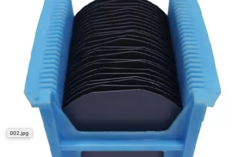
| InP Wafer processing | |
 | |
| Each ingot is cut into wafers which are lapped, polished and surface prepared for epitaxy. The overall process is detailed hereunder. | |
 | |
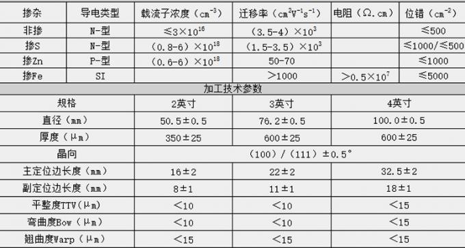
| Flat specification and identification | The orientation is indicated on the wafers by two flats (long flat for orientation, small flat for identification). Usually the E.J. standard (European-Japanese) is used. The alternate flat configuration (U.S.) is mostly used for Ø 4″ wafers. |
| |
| Orientation of the boule | Either exact (100) or misoriented wafers are offered. |
| |
| Accuracy of the orientation of OF | In response to the needs of the optoelectronic industry, we offers wafers with excellent accuracy of the OF orientation : < 0.02 degrees. This feature is an important benefit to customers making edge-emitting lasers and also to manufacturers who cleave to separate dies allowing their designers to reduce the real-estate wasted in the streets. |
| |
| Edge profile | There are two common specs : chemical edge processing or mechanical edge processing (with an edge grinder). |
| |
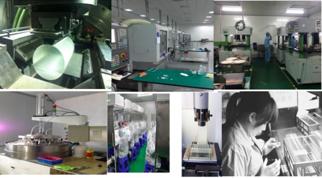
| Polishing | Wafers are polished by means of a chemical-mechanical process resulting in a flat, damage-free surface. we provides both double-side polished and single-side polished (with lapped and etched back side) wafers. |
| |
| Final surface preparation and packaging | Wafers go through many chemical steps to remove the oxide produced during polishing and to create a clean surface with stable and uniform oxide layer that is ready for epitaxial growth – epiready surface and that reduces trace elements to extremely low levels . After final inspection, the wafers are packaged in a way that maintains the surface cleanliness. Specific instructions for oxide removal are available for all types of epitaxial technologies (MOCVD, MBE). |
| |
| Database | As part of our Statistical Process Control/Total Quality Management Program, extensive database recording the electrical and mechanical properties for every ingot as well as crystal quality and surface analysis of wafers are available. At each stage of fabrication, the product is inspected before passing to the next stage to maintain a high level of quality consistency from wafer to wafer and from boule to boule. |
InP Wafer Supplier Shanghai Xinkehui New Material Co. Ltd.

We specialize in processing a varity of materials into wafers, substrates and custiomized optical glass parts.components widely used in electronics, optics, optoelectronics and many other fields. We also have been working closely with many domestic and oversea universities, research institutions and companies, provide customized products and services for their R&D projects.It’s our vision to maintaining a good relationship of cooperation with our all customers by our good reputatiaons.
Send Inquiry
