Semiconductor Crystal Substrate Wafer
2022-09-09
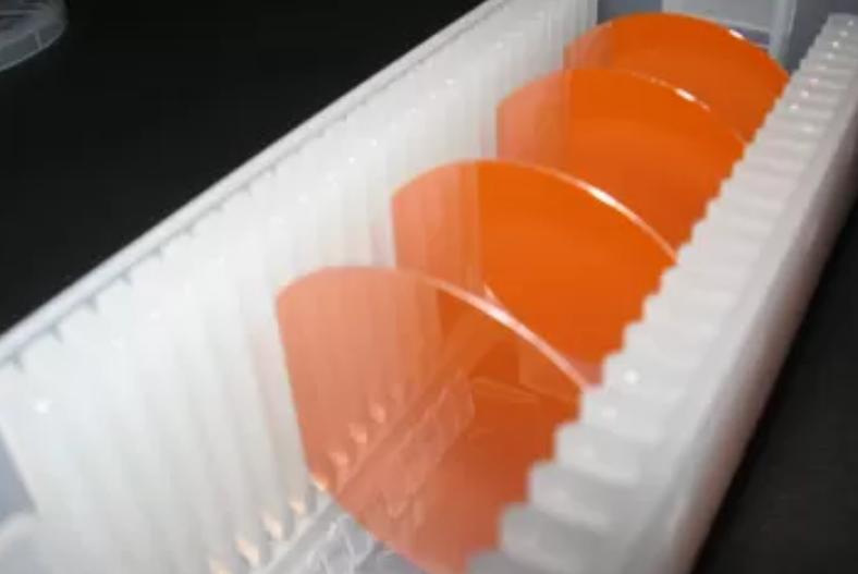
Shanghai Xinkehui New Material have our own factory in Shanghai, China. we can supply the Sapphire, SiC, GaN, GaAs, Silicon and other semiconductor wafers. The Details of our sapphire, SiC, GaN wafer in stock as following:
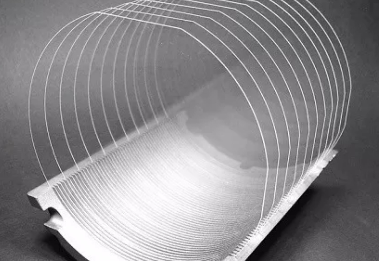
Sapphire Wafer
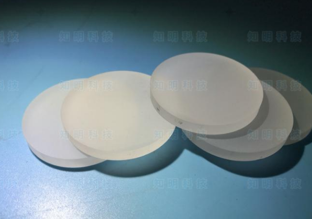
- 2 inch 0.43 mm thickness C-plane DSP/SSP, MOQ 25 pcs;
- 2 inch 0.43 mm thickness A-plane DSP/SSP, MOQ 25 pcs;
- 2 inch 0.43 mm thickness M-plane DSP/SSP, MOQ 25 pcs;
- 2 inch 0.43 mm thickness R-plane DSP/SSP, MOQ 25 pcs;
- 3 inch 0.5 mm thickness C-plane DSP/SSP, MOQ 25 pcs;
- 4 inch 0.65 mm thickness C-plane DSP/SSP, MOQ 25 pcs;
- 6 inch 1.0 mm thickness C-plane DSP/SSP, MOQ 10 pcs;
| GENERAL | ||
| Chemical Formula | Al2O3 | |
| Crystal Stucture | Hexagonal System (hk o 1) | |
| Unit Cell Dimension | a=4.758 Å,Å c=12.991 Å, c:a=2.730 | |
| PHYSICAL | ||
| Metric | English (Imperial) | |
| Density | 3.98 g/cc | 0.144 lb/in3 |
| Hardness | 1525 – 2000 Knoop, 9 mhos | 3700° F |
| Melting Point | 2310 K (2040° C) | |
| STRUCTURAL | ||
| Tensile Strength | 275 MPa to 400 MPa | 40,000 to 58,000 psi |
| Tensile Strength at 20° C | 58,000 psi (design min.) | |
| Tensile Strength at 500° C | 40,000 psi (design min.) | |
| Tensile Strength at 1000° C | 355 MPa | 52,000 psi (design min.) |
| Flexural Stength | 480 MPa to 895 MPa | 70,000 to 130,000 psi |
| Compression Strength | 2.0 GPa (ultimate) | 300,000 psi (ultimate) |
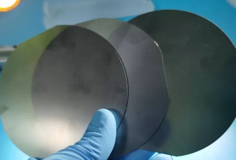
SiC Wafer
- 4 inch 4h-n type 0.35 mm thickness DSP Dummy grade, MOQ 1 pcs;
- 4 inch 4h-n type 0.35 mm thickness DSP Production grade, MOQ 1 pcs;
- 4 inch 4h-n type 0.35 mm thickness DSP Prime Zero grade, MOQ 1 pcs;
- 6 inch 4h-n type 0.35 mm thickness DSP Dummy grade, MOQ 1 pcs;
- 6 inch 4h-n type 0.35 mm thickness DSP Production grade, MOQ 1 pcs;
| Grade | Zero MPD Grade | Production Grade | Research Grade | Dummy Grade |
| Diameter | 100. mm±0.2 mm or other customized size | |||
| Thickness | 1000±25 um Or other customized thickness | |||
| Wafer Orientation | Off axis : 4.0° toward <1120> ±0.5° for 4H-N/4H-SI On axis : <0001>±0.5° for 6H-N/6H-SI/4H-N/4H-SI | |||
| Micropipe Density | ≤0 cm-2 | ≤2 cm-2 | ≤5 cm-2 | ≤30 cm-2 |
| Resistivity 4H-N | 0.015~0.028 Ω•cm | |||
| Resistivity 4/6H-SI | ≥1E7 Ω·cm | |||
| Primary Flat | {10-10}±5.0° or round shape | |||
| Primary Flat Length | 18.5 mm±2.0 mm or round shape | |||
| Secondary Flat Length | 10.0mm±2.0 mm | |||
| Secondary Flat Orientation | Silicon face up: 90° CW. from Prime flat ±5.0° | |||
| Edge exclusion | 1 mm | |||
| TTV/Bow /Warp | ≤10μm /≤10μm /≤15μm | |||
| Roughness | Polish Ra≤1 nm / CMP Ra≤0.5 nm | |||
| Cracks by high intensity light | None | 1 allowed, ≤2 mm | Cumulative length ≤ 10mm, single length≤2mm | |
| Hex Plates by high intensity light | Cumulative area ≤1% | Cumulative area ≤1% | Cumulative area ≤3% | |
| Polytype Areas by high intensity light | None | Cumulative area ≤2% | Cumulative area ≤5% | |
| Scratches by high intensity light | 3 scratches to 1×wafer diameter cumulative length | 5 scratches to 1×wafer diameter cumulative length | 5 scratches to 1×wafer diameter cumulative length | |
| edge chip | None | 3 allowed, ≤0.5 mm each | 5 allowed, ≤1 mm each |
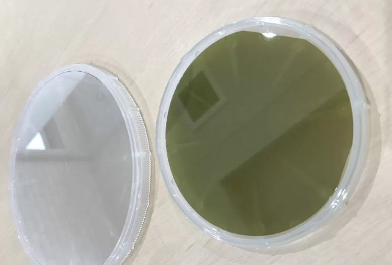
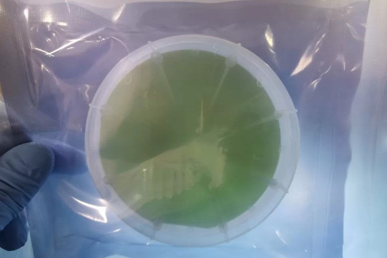
GaN Wafer
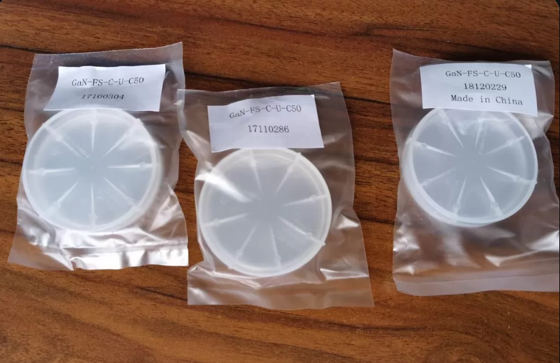
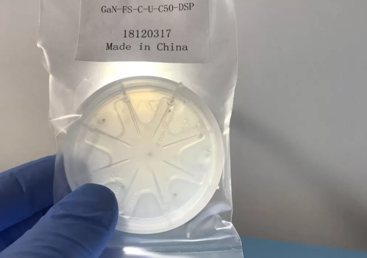
- 2inch Free-standing HVPE GaN substrate 0.4 mm thickness DSP Dummy grade, MOQ 1 pcs;
- 2inch Free-standing HVPE GaN substrate 0.4 mm thickness DSP Research grade, MOQ 1 pcs;
| Free-standing GaN Substrates (2”) | |
| Item | JF-261NA-M3/JF-261NA-A2 |
| Size(mm) | 50.0±0.5 |
| Thickness(um) | 400±25 |
| TTV(um) | ≤15 |
| BOW(um) | ≤20 |
| RMS(nm) | Ga face:RMS,0.2 nm(10um*10um);N face: Lapped and etched |
| Orientation | C-plane(0001) off angle toward M-axis/A-axis 0.3±0.25 |
| Conduction Type | Doped N-type |
| Resistivity (Ω.cm) | ≤0.05 |
| Carrier Concentration(cm∧-3) | ≥1*10∧18 |
| Dislocation Density(cm∧-2) | ≤5*10∧6 |
| FWHM(arcsec) | ≤120 |
| Useable Surface Area | >90% |
Related Semiconductor Products
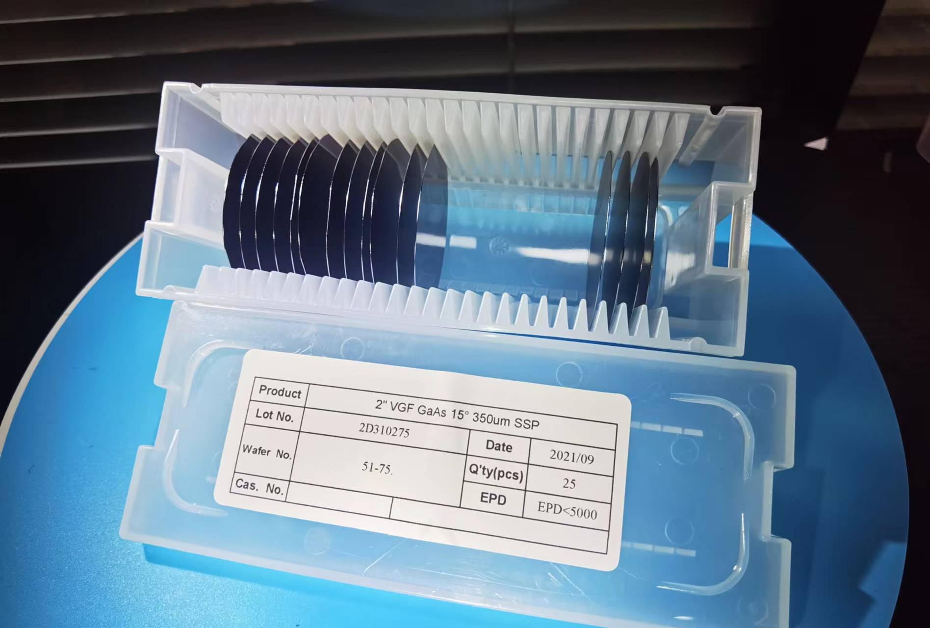
besides the sapphire,SiC,GaN, we also can supply GaAs, silicon, GaP…
Shanghai Xinkehui New Material
———-professional semiconductor wafer supplier

Shanghai Xinkehui New Material Co., Ltd. is a high-tech company specializing in semiconductor materials such as sapphire substrates, sapphire wafers, sic substrates, and silicon wafers.Annual sales of 20 million RMB, Our company was established in 2016 and currently serves more than 50 countries and regions around the world.