

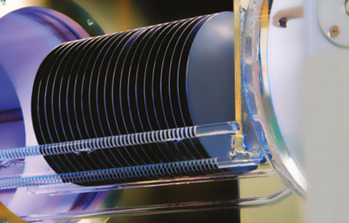
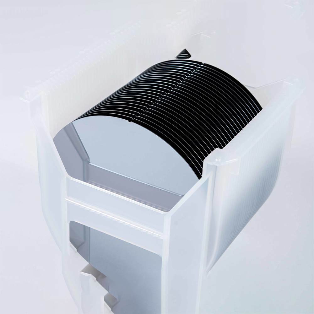
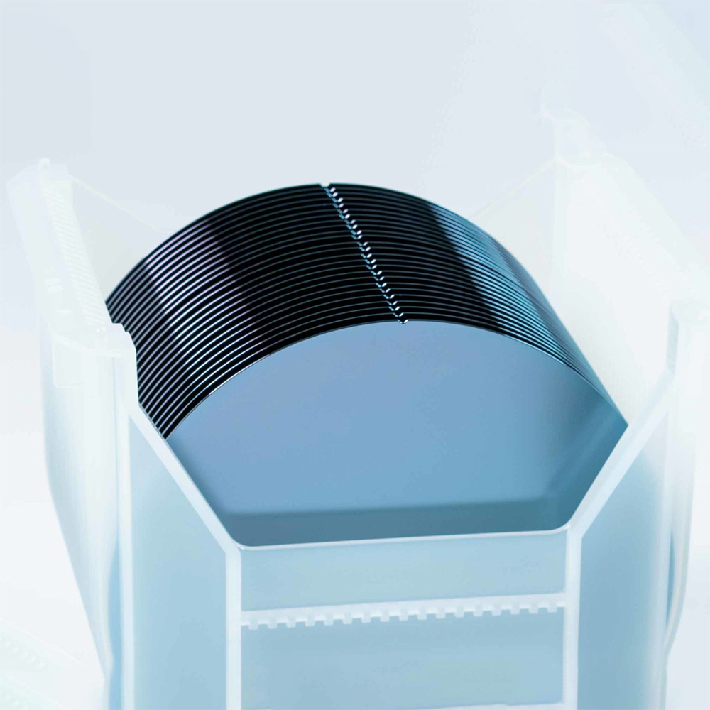
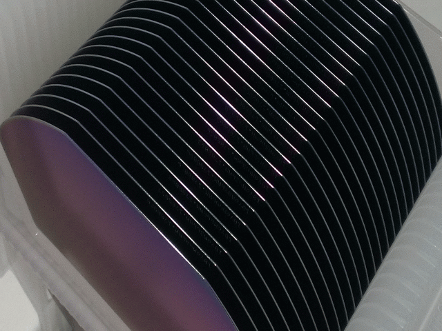
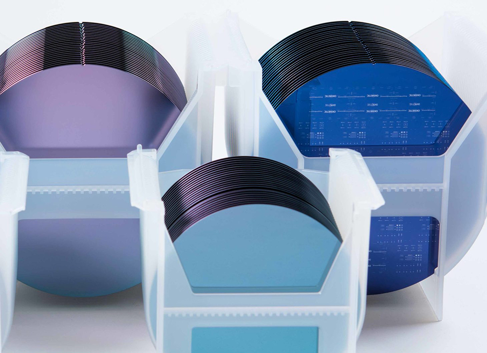
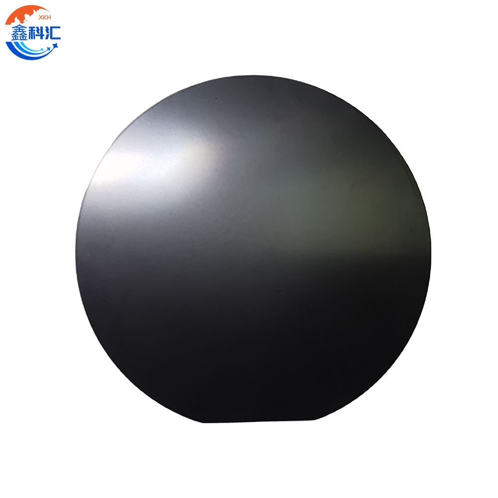
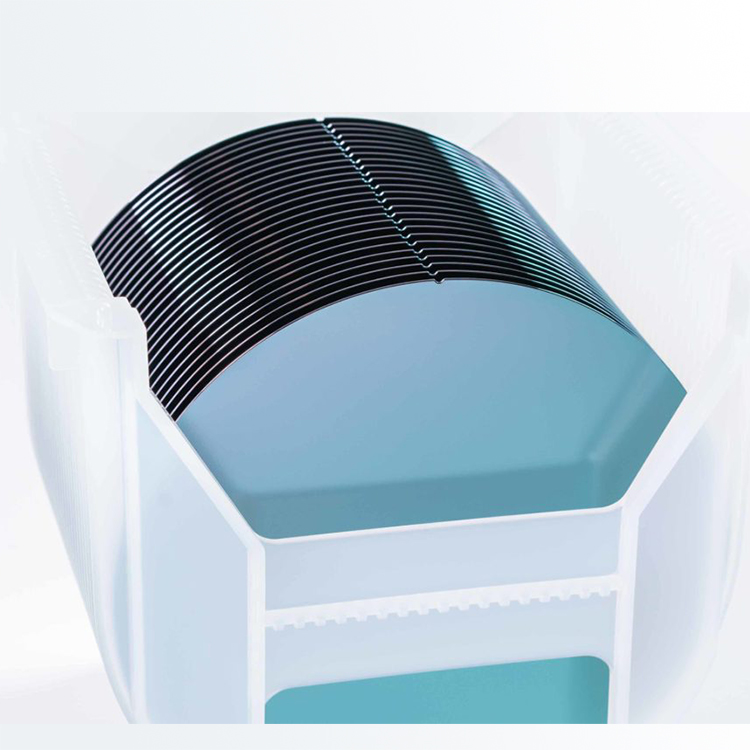
SOI Wafer Silicon On Insulator Semiconductor Wafer
SOI Wafer sizes from 3” to 200mm, some in inventory Ver […]
Send Inquiry
Add To Cart
- SOI Wafer sizes from 3” to 200mm, some in inventory
- Very high quality with tight TTV on device layer thickness
- Direct Si-Si bonding and double sided SOI available
- Any Si orientation, any device thickness over 1.5um
- Single and double side polished
- Small lot sizes and Laser marking of wafers available
- Short lead time delivery
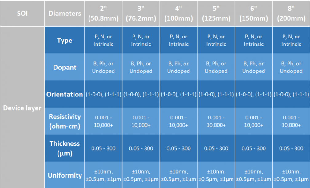
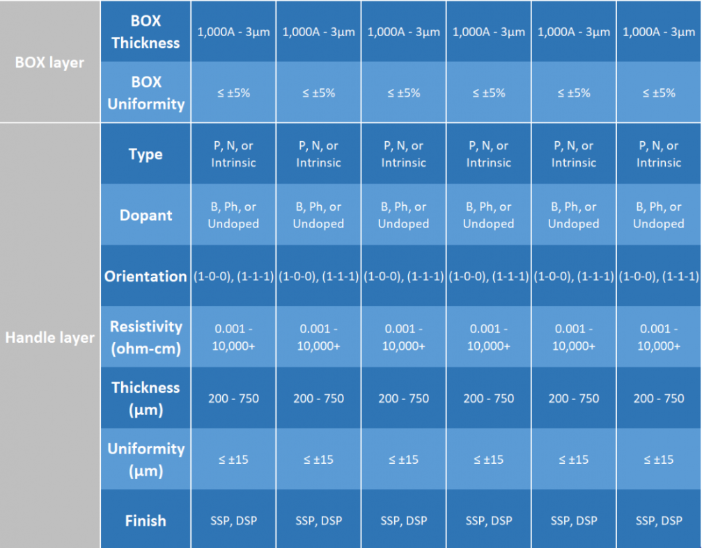
Product Specification
| Method | Fusion bonding |
|---|---|
| Diameter | Ø 4″/ Ø 6″ / Ø 8″ |
| Device thickness | 2 um ~ 300 um |
| Tolerance | +/- 0.5 um ~ 2 um |
| Orientation | <100> / <111> / <110> or others |
| Conductivity | P – type / N – type / Intrinsic |
| Dopant | Boron / Phosphorous / Antimony / Arsenic |
| Resistivity | 0.001 ~ 100000 ohm-cm |
| Oxide thickness | 500A ~ 4 um |
| Tolerance | +/- 5% |
| Handle wafer | >= 300 um |
| Surface | Double sides polished |
| Coating | Oxide and nitride can be supplied on both sides of SOI wafer |
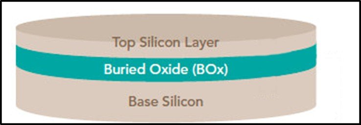
SOI wafers are offered with great customizability and the parameters are greatly flexible as per your needs.
Send Inquiry
